Manufacturing method for silicon single crystal

A manufacturing method, silicon single crystal technology, applied in the direction of single crystal growth, single crystal growth, chemical instruments and methods, etc., can solve the problems of complicated setting of cultivation conditions, etc.

Active Publication Date: 2019-07-12
SUMCO CORP
View PDF6 Cites 1 Cited by
  • Summary
  • Abstract
  • Description
  • Claims
  • Application Information

AI Technical Summary

Problems solved by technology

[0004] However, in the technique described in the aforementioned Document 1, it is necessary to measure various parameters during the growth of the silicon single crystal, analyze the measurement results by multivariate analysis, and adjust the doping in the next growt

Method used


Image

  • Manufacturing method for silicon single crystal
  • Manufacturing method for silicon single crystal
  • Manufacturing method for silicon single crystal

Examples


Embodiment

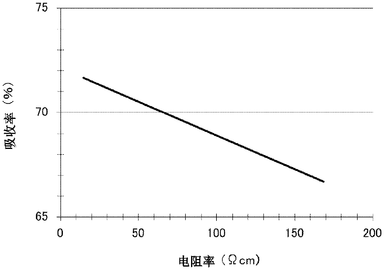
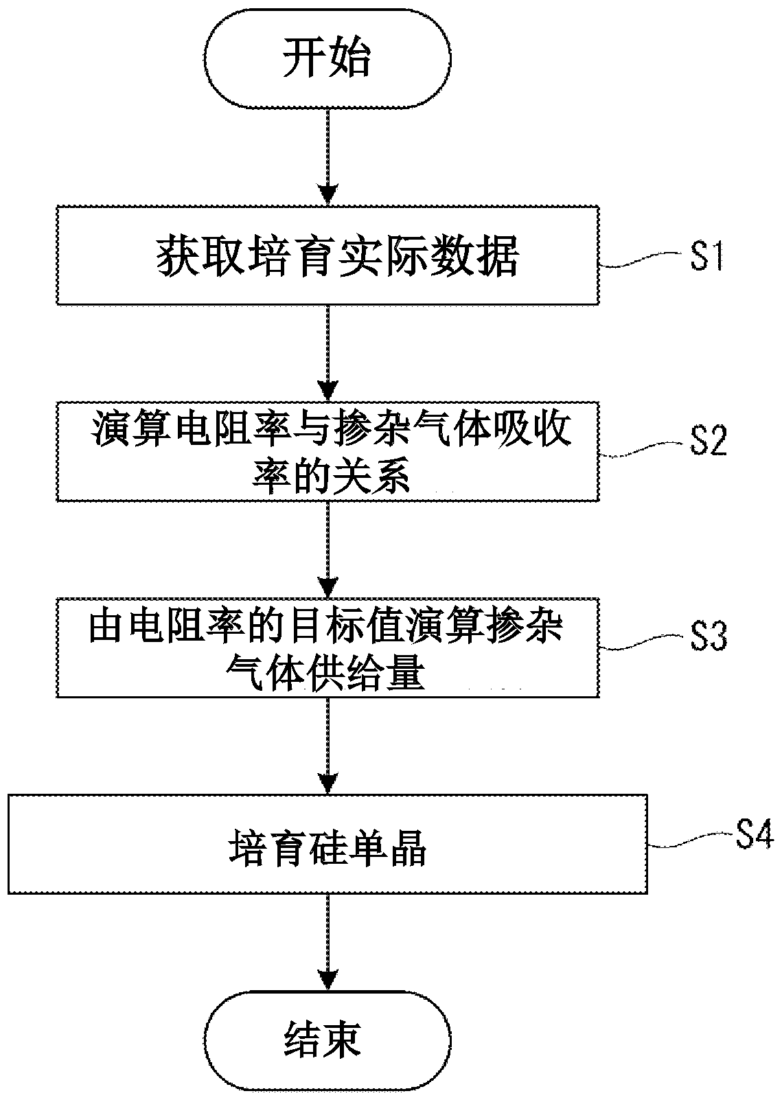
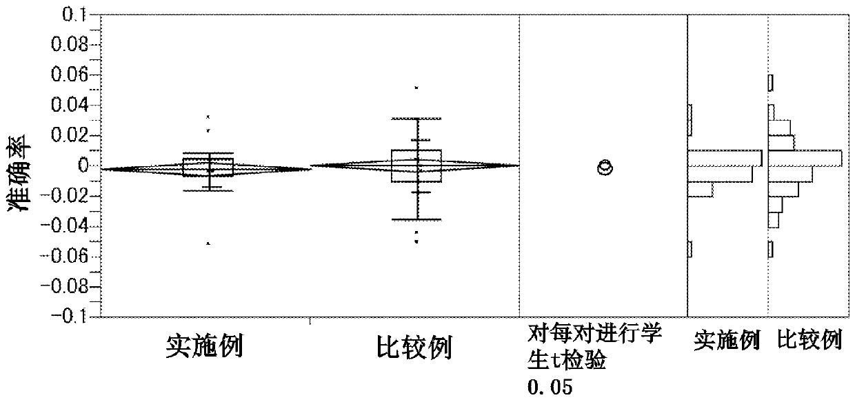
[0067] As described in the foregoing embodiment, the relationship between the measured electrical resistivity and the dopant gas absorptivity is calculated in the second step based on the actual cultivation data in the first step, and in the third step, the calculated dopant gas absorptivity , set the dopant gas flow rate in the next cultivation, and compare the above-mentioned scheme (example) with the situation that the dopant gas absorption rate of the previous time is kept constant (comparative example). It should be noted that the difference between the example and the comparative example is only the flow rate of the doping gas, and other processing conditions are the same.

[0068] A specific comparison method evaluates whether or not the actual value of the resistivity of the grown silicon single crystal 3 varies to some extent with respect to the target value of the resistivity as a variation in accuracy. That is, the accuracy rate is given by the following formula (3)...


PUM


Abstract

Disclosed is a manufacturing method for a silicon single crystal, in which the silicon single crystal is grown by an FZ method for controlling the resistivity while blowing a dopant gas into a moltenband region. The method comprises the steps: (S1) acquiring actual data for growing the silicon single crystal by means of a prescribed growing device; step (S2), based on the cultivation actual data,calculating the relationship between the actual value of the resistivity of the silicon single crystal and the doping gas absorption rate of the silicon single crystal; (S3) calculating the amount ofdoped gas supplied on the basis of the relationship between the actual value of the resistivity and the absorption rate of the doped gas and the target value of the resistivity of the silicon singlecrystal manufactured using the same cultivation device; (S4) controlling the resistivity of the cultured silicon single crystal while blowing the dopant gas by using the calculated dopant gas supply amount.

Description

technical field [0001] The present invention relates to a method for manufacturing silicon single crystals. Background technique [0002] The FZ (Floating Zone, floating zone) method melts polycrystalline raw materials with high resistivity, and blows phosphorus (PH 3 ), boron (B 2 h 6 ) and other doping gases to control the resistivity, thereby growing silicon single crystals. In order to control the resistivity of a silicon single crystal, it is necessary to perform growth control while taking various conditions of the thermal field into consideration. [0003] Therefore, Document 1 (Japanese Unexamined Patent Publication No. 2015-101521 ) discloses a technique of measuring the neck diameter and the melt diameter during the growth of a silicon single crystal in a method for producing a silicon single crystal by the FZ method. , region length, crystal temperature, upper axis speed and other parameters that affect the resistivity, and cultivate silicon single crystal tec...

Claims


Application Information

Patent Timeline
IPC IPC(8): C30B29/06C30B13/12C30B13/28
CPCC30B29/06C30B13/12C30B13/28
Inventor 铃木优作
Owner SUMCO CORP
Why Eureka
Try Eureka