Linear array camera and area array camera combined large-aperture super clean smooth surface defect detection device

A technology for smooth surface and defect detection, which is applied in measuring devices, optical testing of flaws/defects, and material analysis through optical means. It can solve the problems of inability to meet the requirements of detection speed, low detection efficiency and production capacity, and differences in photosensitivity. , achieve fast scanning speed, increase industrial production output, and detect sensitive effects

Active Publication Date: 2019-07-12
HANGZHOU JINGNAIKE OPTOELECTRONICS TECH CO LTD
View PDF7 Cites 19 Cited by
  • Summary
  • Abstract
  • Description
  • Claims
  • Application Information

AI Technical Summary

Problems solved by technology

However, with the increase of the caliber of smooth surface components, the traditional low-magnification scanning method based on area array cameras must pause to collect a frame of images to ensure that clear images can be collected in a stable state, so the speed is very slow and has gradually failed to meet Requirements for detection speed in the field, low detection efficiency and production capacity
At the same time, the original area array camera often adopts a large-format area array camera spliced ​​by multiple CCDs, so that the photosensitivity of different areas on the image is different.
In addition, during the scanning of large-diameter components, it is necessary to ensure that the entire surface is within the focus range of the imaging system, otherwise a clear image will not be obtained, which poses a high challenge to the attitude adjustment of the component and the focusing ability of the imaging system. requirements, especially for components with high cleanliness and smooth surfaces, the surface has no features, and even the detection environment is controlled even with dust, so the traditional autofocus algorithm based on image features is difficult to work

Method used


Image

  • Linear array camera and area array camera combined large-aperture super clean smooth surface defect detection device
  • Linear array camera and area array camera combined large-aperture super clean smooth surface defect detection device
  • Linear array camera and area array camera combined large-aperture super clean smooth surface defect detection device

Examples


Embodiment 1

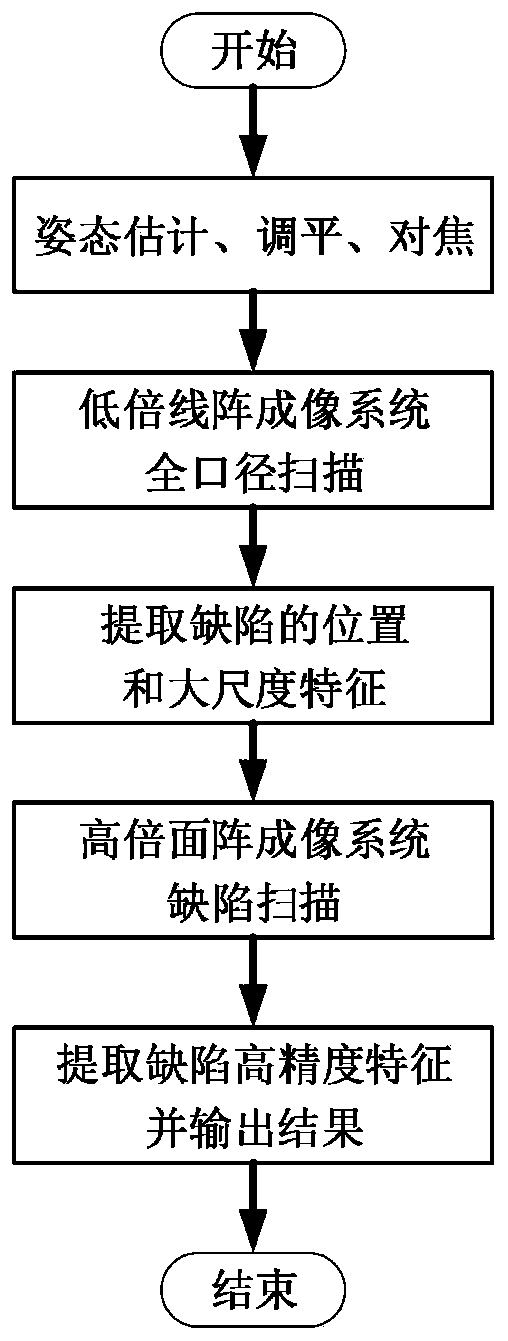
[0028] Below, embodiment 1 of the present invention will use Figure 1-7 to describe in detail.

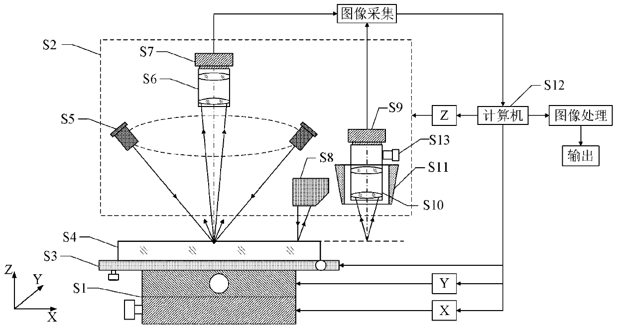
[0029] Such as figure 1As shown, a large-caliber ultra-clean smooth surface defect detection device combined with a line array camera, including a low-magnification linear array imaging system, a high-magnification area array imaging system, a distance sensing system S8, an XY two-dimensional guide rail S1, and a Z guide rail S2, clamping table S3 and console S12. Among them, the low-magnification linear array imaging system is used to quickly collect defect information on large-diameter surfaces. It consists of a ring-shaped illumination source S5, a low-magnification linear array lens S6, and a linear array camera S7. The magnification of the optical system is 1.4 times The ring-shaped lighting source S5 adopts multi-beams of high-brightness and high-uniform white LEDs distributed in a ring, obliquely incident on the ultra-clean smooth surface sample S4 at a specific angle, wh...


PUM


Abstract

The invention discloses a linear array camera and area array camera combined large-aperture super clean smooth surface defect detection device. When a super clean smooth surface is detected, the device provided by the invention firstly uses a linear array camera with low magnification factor to quickly scan full aperture and acquires a dark field image of a sample surface, extracts position information of defects, and then, locates each defect through an area array camera configured with a high fixed-times optical system and further performs data processing analysis for the image, and thus, obtains a high-precision detection result. Such detection mode is not only fast, but also highly accurate and sensitive. Moreover, the device provided by the invention also carries a distance sensing system for leveling of a to-be-detected super clean smooth surface and focusing of an imaging system, and has more fast adjustment accuracy and stability. The device provided by the invention solves a difficult problem of various large-aperture super clean smooth surface defect automated detection, and can be used for fast detection on surfaces of various smooth glass, wafers, metals and so on.

Description

technical field [0001] The invention belongs to the technical field of machine vision detection, and provides a large-diameter ultra-clean smooth surface defect detection device combined with a line array camera, in particular to a fast large-diameter ultra-clean smooth surface defect detection device combined with a line array camera and method. Background technique [0002] In the fields of advanced optical component manufacturing and semiconductor industry, automatic quantitative detection of defects on smooth surfaces such as smooth glass, semiconductor wafers, and metals is an important link in component quality control and process monitoring. The digital quantitative detection of smooth surface defects will provide a powerful means to ensure the factory quality of components and improve the production capacity of industrial production. At present, the original surface defect detection system uses a variable magnification microscopic imaging device to balance the perfo...

Claims


Application Information

Patent Timeline
Patent Type & Authority Applications(China)
IPC IPC(8): G01N21/88
CPCG01N21/8806G01N21/8851G01N2021/8874G01N2021/8887
Inventor 杨甬英曹频
Owner HANGZHOU JINGNAIKE OPTOELECTRONICS TECH CO LTD
Why Eureka
Try Eureka