Low-power consumption boundary scanning test method

A technology of boundary scan testing and boundary scan, which is applied in the direction of electronic circuit testing, measuring electronics, measuring devices, etc., and can solve problems affecting test results, etc.

Active Publication Date: 2019-07-12
HARBIN INST OF TECH AT WEIHAI
View PDF8 Cites 7 Cited by
  • Summary
  • Abstract
  • Description
  • Claims
  • Application Information

AI Technical Summary

Problems solved by technology

[0005] The purpose of the present invention is to solve the problem that the existing low-power boundary-scan test method affects the test results at the expense of fault coverage, and provides a low-power boundary-scan test method

Method used


Image

  • Low-power consumption boundary scanning test method
  • Low-power consumption boundary scanning test method
  • Low-power consumption boundary scanning test method

Examples


specific Embodiment approach 1

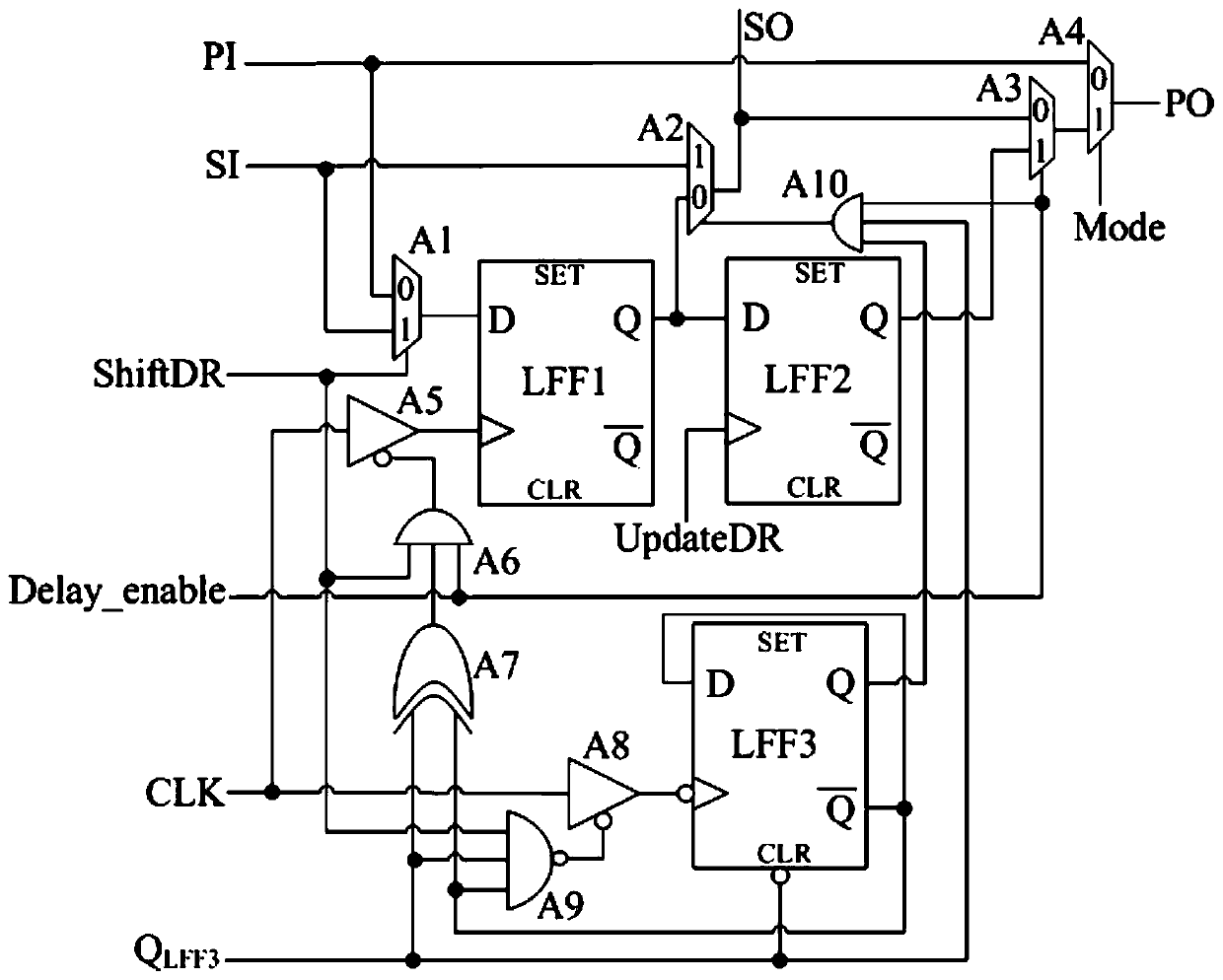
[0078] Specific implementation mode 1. In the non-delay test mode, the specific working process of the input boundary scan chain:

[0079] Capture phase: see Figure 5(a), Delay_enable is 1, CLK is the test clock; ShiftDR is 0, and the initial value 0 is set to the D flip-flop LFF3; at the same time, control the tri-state gate A5 of the LFF1 clock terminal (active low) is turned on, BSCC1 can capture the response of the previous test process into LFF1 through the system input terminal PI under the trigger of the clock.

[0080] Shift phase: See Figure 5(b). When the control signal ShiftDR changes from 0 to 1, the test enters the shift phase, and at the same time, the tri-state gate A8 that controls the LFF3 clock terminal in BSLC1 is opened. The test vector is sequentially input from the test serial input terminal SI bit by bit. When the rising edge of the first test clock arrives, the first bit of the test vector is shifted into LFF1 of BSLC1. When the falling edge of the fir...

specific Embodiment approach 2

[0088] Specific implementation mode 2. In the full-speed test mode, the specific working process of the input boundary scan chain:

[0089] In full-speed testing, the boundary-scan cell skips the capture phase and goes directly to the shift phase, which moves the test vectors into the scan chain. After the shift is completed, the Delay_enable signal changes from 1 to 0, and the scanning unit enters the full-speed test mode.

[0090] Specifically: the initial Delay_enable is 1, CLK is the test clock; perform a shift to move the test vector into the scan chain;

[0091] After the shift is completed, the Delay_enable signal changes from 1 to 0, and the input clock is switched to the functional clock. At the same time, the test vector is applied to the functional path through the PO terminal of the BSLC scanning unit as its initial logic value;

[0092] When the first rising edge of the function clock arrives, the scan chain performs another shift, and the logic value conversion ...

specific Embodiment approach 3

[0097] Specific embodiment three, combine Figure 7-10 This embodiment will be described, and simulation experiment data will be given in this embodiment.

[0098] In order to verify whether the present invention can correctly complete operations in different test phases such as shift, capture, and update and reduce test power consumption, we perform functional simulation on a boundary-scan unit with low test power consumption. In the experiment, 16 boundary scan units are used to form a scan chain to simulate the test vector shift process, including 8 emission units and 8 capture units. The test clock frequency is set to 100MHz. It is worth noting that the PI-side input signal and PO-side output signal mentioned in the experiment are two 16-bit signals, which are the test vector SI_LC and the test response SO_CC, which represent the system input and output ports PI and PO in the boundary scan unit. the value of figure 1 The data values ​​at PI and PO marked in ; SOi repres...


PUM


Abstract

The invention discloses a low-power consumption boundary scanning test method, belongs to the field of SOC boundary scanning test, and aims at solving the problem that the existing low-power consumption boundary scanning test methods are at the cost of sacrificing the fault coverage rate so that the test results are influenced. According to the method, the output end of each chip on an SOC is connected with a BSLC scanning unit; the SI ends and SO ends of every two adjacent boundary scanning units in n BSLC scanning units are sequentially connected in series to form an input boundary scanningchain which is used for sending test excitations to a function path; the input end of each chip is connected with a BSCC scanning unit; the SI ends and SO ends of every two adjacent boundary scanningunits in m BSCC scanning units are sequentially connected in series to form an output boundary scanning chain which is used for capturing and moving test responses; and when each bit of test data is moved in, the state of a trigger on the whole scanning chain is switched for less than twice, so that the test power consumption is greatly decreased.

Description

technical field [0001] The invention belongs to the field of SOC boundary scan test, in particular to a low power consumption boundary scan unit structure. Background technique [0002] The emergence of deep submicron and nanometer process technology of integrated circuits has realized the integration of a complete circuit system on a chip, which constitutes a system on a chip (System On a Chip, SOC) based on IP core multiplexing. At present, SOC has been widely used in aerospace, military electronic systems, Internet, multimedia systems and other fields by virtue of many advantages such as high performance, small size, and short development cycle. [0003] A large number of modules or IP cores with different functions are integrated in the SOC. With the continuous improvement of circuit complexity and operating speed, and the continuous reduction of transistor feature size, the possible faults in the chip increase sharply, and the test complexity and difficulty also increas...

Claims


Application Information

Patent Timeline
IPC IPC(8): G01R31/28
CPCG01R31/2856
Inventor 邓立宝付宁乔立岩孙宁彭喜元
Owner HARBIN INST OF TECH AT WEIHAI
Why Eureka
Try Eureka