Method and device for detecting thickness of film

A technology for detecting thin films and thin films, applied in measuring devices, instruments, using wave/particle radiation, etc., can solve problems such as inability to measure, unsuitable for measuring metal and alloy thin films, etc.

Inactive Publication Date: 2019-07-16
ZHEJIANG SHANGFANG ELECTRONICS EQUIP +1
View PDF13 Cites 6 Cited by
  • Summary
  • Abstract
  • Description
  • Claims
  • Application Information

AI Technical Summary

Problems solved by technology

Although the ellipsometer method can measure the thickness of films with a thickness of 1nm or less, it is generally not suitable for measuring metal and alloy films and other opaque films.
Photoelectron spectroscopy and Auger electron spectroscopy can also obtain information on the surface of materials, but they can only obtain in...

Method used


Image

  • Method and device for detecting thickness of film
  • Method and device for detecting thickness of film
  • Method and device for detecting thickness of film

Examples


Embodiment 1

[0070] Embodiment 1 Substrate signal attenuation method

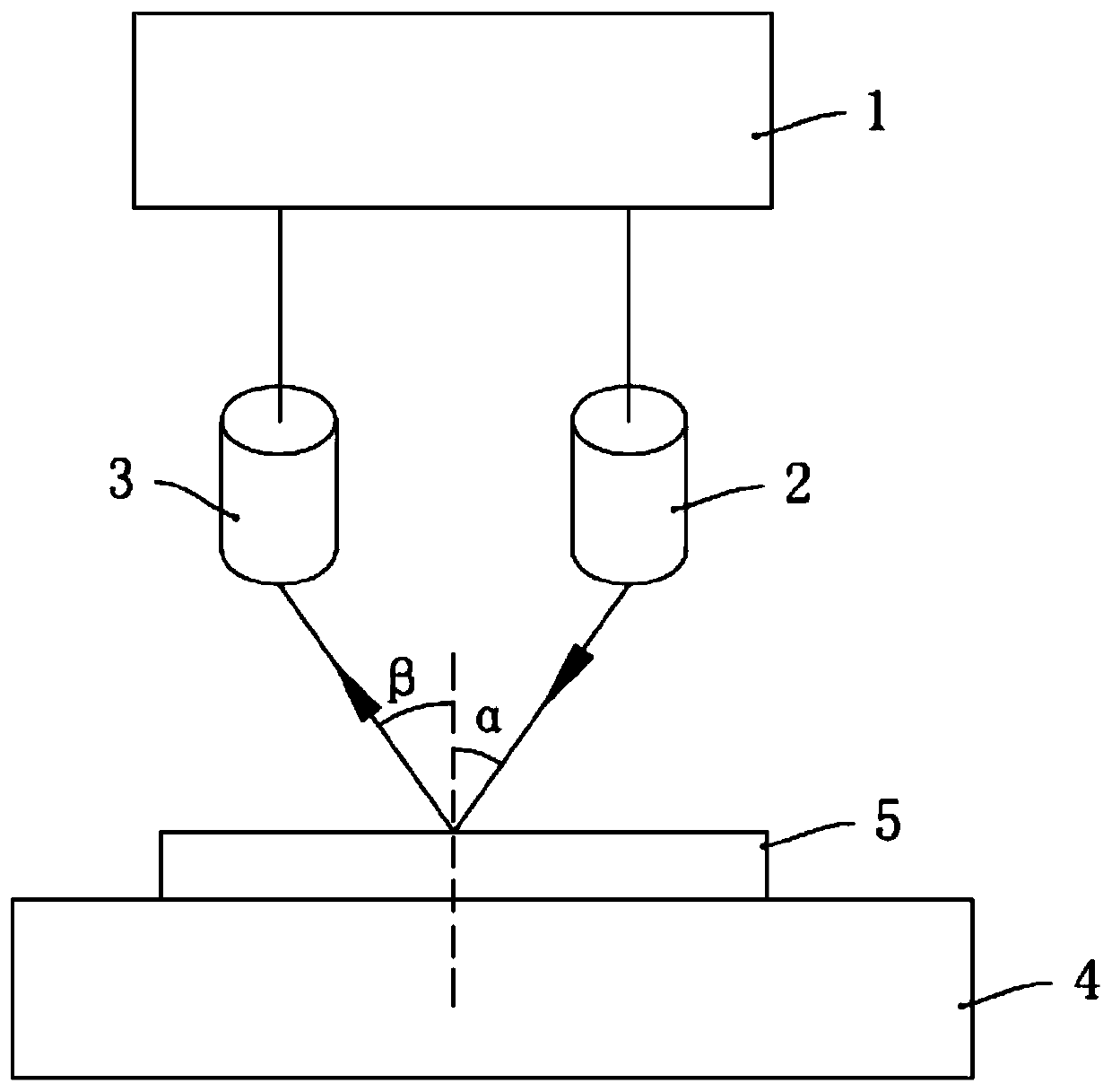
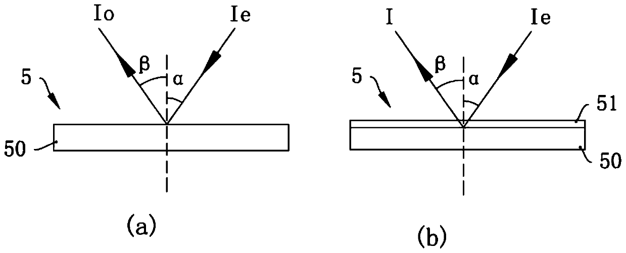
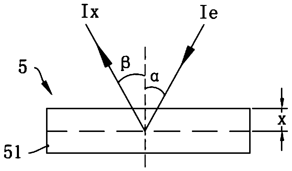
[0071] Place the silicon substrate without film deposition and the samples deposited with aluminum films of different thicknesses on the test platform 4 respectively, and keep the ambient air pressure lower than 5×10 -4 Pa, the electron beam generating device 2 generates electron beams to project on each sample in turn, the energy of the electron beam is 2keV, and the beam current is 50nA, and the detection device 3 obtains the EDS energy spectrum of each sample, as Figure 4 shown. The X-ray fluorescence characteristic energy corresponding to the substrate Si element is 1.739keV. Such as Figure 5 As shown, with the increase of Al film thickness, the intensity of X-ray fluorescence characteristic energy corresponding to Si element decreases gradually.

[0072] For the substrate Si signal, the intensity exhibits an exponential decay characteristic with the increase of Al film thickness. Exponential fitting (implemen...

Embodiment 2

[0074] Embodiment 2 thin film signal enhancement method

[0075] Place the silicon substrate without film deposition and the samples deposited with aluminum films of different thicknesses on the test platform 4 respectively, and keep the ambient air pressure lower than 5×10 -4 Pa, the electron beam generating device 2 generates electron beams to project on each sample in turn, the energy of the electron beam is 2keV, the beam current is 50nA, and the detection device 3 obtains the X-ray fluorescence energy spectrum corresponding to the Al element whose characteristic energy of each sample is 1.485keV ,Such as Figure 4 shown. As the thickness of the Al film increases, the intensity of the X-ray fluorescence characteristic energy corresponding to the Al element increases gradually.

[0076] For the Al signal in thin films, the intensity shows an exponential increase characteristic with the increase of Al film thickness, see Figure 7 . Exponential fitting (implemented in th...


PUM


Abstract

The invention discloses a method and device for detecting the thickness of a film. The method comprises the following steps that electron beams with the same energy and the same strength are projectedto a reference sample and a to-be-detected sample, and the samples are excited to emit X-ray fluorescence; the strength of X-ray fluorescence characteristic energy corresponding to target elements inthe two samples is collected; the thickness of the film is calculated according to a relational expression between the ratio of the two pieces of strength and the thickness of the film; when a blanksubstrate is adopted as the reference sample, the strength of X-ray fluorescence characteristic energy corresponding to a target element in the substrate is collected; and when a block standard samplemade of the same material as the film is adopted as the reference sample, the strength of X-ray fluorescence characteristic energy corresponding to a target element in the substrate is collected. Themethod and device for detecting the thickness of the film adapt to measurement of the thickness within the large range of 0.1 nm to 100 nm by adjusting the energy and the angles of the incident electron beams.

Description

technical field [0001] The invention relates to the technical field of thin film detection, in particular to a method and device suitable for detecting the thickness of a nanoscale thin film. Background technique [0002] Thin films have been widely used in optoelectronic devices, and their thickness is an important parameter, which has an important impact on the optoelectronic properties of devices. Furthermore, due to the high cost of making photoelectric thin films, it is required that the measurement must be non-destructive. There are many methods for non-destructive measurement of film thickness, such as optical interferometry, X-ray fluorescence spectroscopy, ellipsometer method, photoelectron spectroscopy and Auger electron spectroscopy, quartz crystal oscillator method, small-angle X-ray diffraction method and high-resolution X-ray diffraction rocking curve method, etc. [0003] Optical interferometry is only suitable for the measurement of thickness above 10nm, an...

Claims


Application Information

Patent Timeline
IPC IPC(8): G01B15/02
CPCG01B15/02
Inventor 周海龙季振国俞峰张永夫丁靓蔡好
Owner ZHEJIANG SHANGFANG ELECTRONICS EQUIP
Why Eureka
Try Eureka