Integrated circuit protection structure and manufacturing method thereof

A technology for protecting structures and integrated circuits, applied in circuits, electrical components, electrical solid devices, etc., can solve problems such as affecting the process, failure to fill the upper layer of conductive via holes, invalid protection structures, etc., and achieve the effect of preventing damage or peeling

Active Publication Date: 2020-07-31
YANGTZE MEMORY TECH CO LTD
View PDF6 Cites 0 Cited by
  • Summary
  • Abstract
  • Description
  • Claims
  • Application Information

AI Technical Summary

Problems solved by technology

[0005] In view of the above-mentioned shortcomings of the prior art, the purpose of the present invention is to provide a protective structure for integrated circuits, which is used to solve the phenomenon of holes in the lower conductive part in the prior art, which easily leads to the failure of filling the upper conductive via holes, making the protection structure invalid , and affect subsequent process issues

Method used


Image

  • Integrated circuit protection structure and manufacturing method thereof
  • Integrated circuit protection structure and manufacturing method thereof
  • Integrated circuit protection structure and manufacturing method thereof

Examples


Embodiment 1

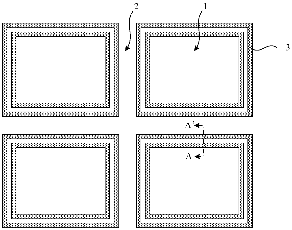
[0067] In this embodiment, the sealing ring is taken as an example to illustrate the integrated circuit protection structure of the present invention. In other embodiments, the integrated circuit protection structure may also be a protection ring or other protection structures.

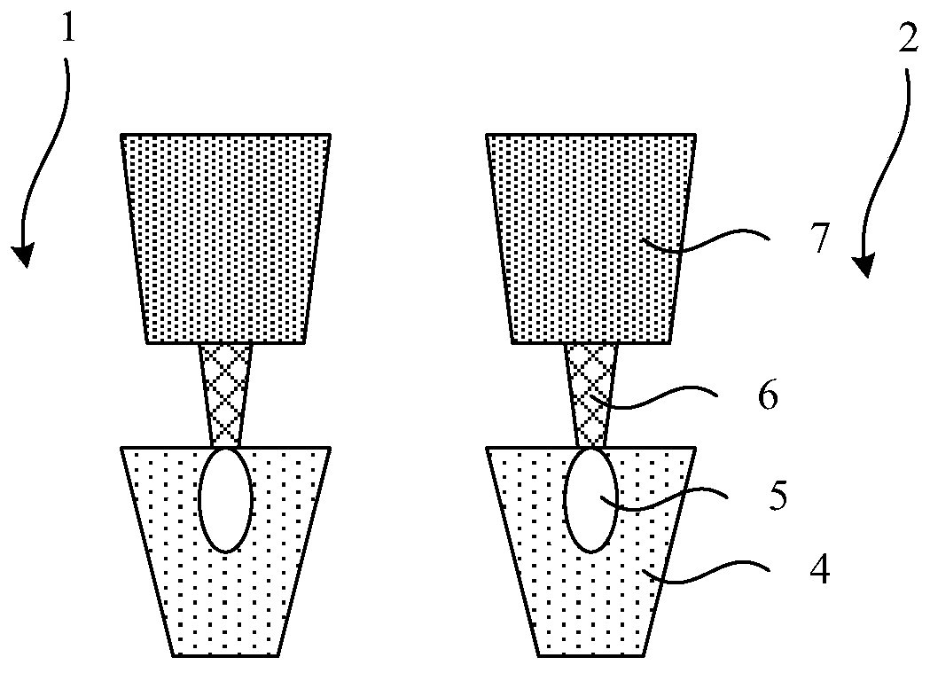
[0068] see Figure 4 , shown as the A-A' direction of the seal ring structure (see figure 1 The cross-sectional view indicated by the two-way arrow in the center), in which, figure 1 Each set of sealing rings only shows two ring structures, while Figure 4 The ellipsis in represents that the number of ring structures in the seal ring structure is not limited to two rings, and can be more.

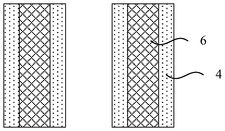
[0069] Specifically, the annular structure includes a first interconnection layer, a via layer and a second interconnection layer, wherein the first interconnection layer includes at least one conductive portion 4, and the via layer includes at least one conductive portion 4. A via 6, the conductive via 6 is con...

Embodiment 2

[0079] This embodiment adopts basically the same technical solution as that of Embodiment 1, the difference is that in Embodiment 1, the conductive vias deviate from the center of the lower conductive part toward the inner side of the annular structure, while in this embodiment, each The conductive via holes of the ring structure are all deviated from the center of the lower conductive portion 4 toward the outside of the ring structure.

[0080] see Figure 6 and Figure 7 ,in, Figure 6 It is shown as an A-A' sectional view of the seal ring structure in this embodiment. Figure 7 shown as Figure 6 The relative top view of the conductive portion 4 and the conductive via 6 in the shown structure.

Embodiment 3

[0082] This embodiment adopts basically the same technical solution as that of Embodiment 1, the difference is that in Embodiment 1, the conductive vias deviate from the center of the lower conductive part towards the inner side of the annular structure, while in this embodiment, at least One of the conductive vias 6 of the annular structure deviates from the center of the lower conductive part 4 toward the inner side of the annular structure, and at least one of the conductive vias 6 of the annular structure goes toward the inner side of the annular structure. The outer direction of the outer layer deviates from the center of the lower layer conductive part 4 .

[0083] see Figure 8 and Figure 9 , it is shown that the conductive via hole 6 of the inner ring structure deviates from the center of the lower conductive part 4 toward the outer direction of the ring structure, and the conductive through hole 6 of the outer ring structure deviates toward the inner direction of th...


PUM


Abstract

The invention provides an integrated circuit protection structure and a manufacturing method thereof. The integrated circuit protection structure comprises at least one ring of annular structure, wherein the annular structure comprises a first interconnection layer, a through hole layer and a second interconnection layer, wherein the first interconnection layer comprises at least one conductive part; the through hole layer comprises at least one conductive through hole, wherein the conductive through hole is connected to the upper portion of the conductive part, and the center of the conductive through hole deviates from the center of the conductive part; and the second interconnection layer comprises at least one conductive wire, wherein the conductive wire is connected above the conductive through hole. The asymmetric design is adopted for the axial symmetric design, wherein the center of the conductive through hole is deviated from the center of the lower-layer conductive part through transverse displacement, so that the conductive through hole completely or partially avoids the part of a hole of the lower conductive part, the conductive through hole can be effectively filled, the high-quality and reliable functions of a sealing ring, a protection ring and the like are facilitated, and influence to the later process is avoided. In addition, by adopting the scheme of the invention, the additional process cost is not increased.

Description

technical field [0001] The invention belongs to the field of semiconductor integrated circuits, and relates to an integrated circuit protection structure and a manufacturing method thereof. Background technique [0002] For the current three-dimensional NAND flash (3D-NAND) technology, an effective seal ring (SR) structure can provide a hermetic seal to isolate moisture and protect the die from mechanical damage during dicing. Current process flows for seal ring formation may include photolithography, trench etching, metal filling, and chemical mechanical polishing (CMP). [0003] The high aspect ratio of the contact array (CTA) of the seal ring makes the etch and metal filling process difficult to control, easily forming a void in the center of the seal ring. Some contact array voids of the seal ring will be exposed after the CMP process, which can easily trap slurries and chemicals, and this side effect will cause seal ring ineffectiveness and yield loss. The current des...

Claims


Application Information

Patent Timeline
Patent Type & Authority Patents(China)
IPC IPC(8): H01L23/48H01L23/528H01L23/02H01L21/768
CPCH01L21/76805H01L21/76838H01L23/02H01L23/481H01L23/528H01L23/5283
Inventor 肖金华范鲁明彭进郑祖辉
Owner YANGTZE MEMORY TECH CO LTD
Why Eureka
Try Eureka