Aluminum-lithium alloy solid-state ion conduction layer and preparation method thereof and full-solid-state electrochromic device containing solid-state ion conduction layer
An electrochromic device and ion conduction layer technology, applied in the field of applications and materials, can solve the problems of long preparation time, low sputtering rate, ion mutual diffusion loss, etc. drain effect
- Summary
- Abstract
- Description
- Claims
- Application Information
AI Technical Summary
Problems solved by technology
Method used
Image
Examples
Embodiment 1
[0054] Clean the glass substrate, put it into the magnetron sputtering equipment, and sputter to form a transparent conductive material: the target material is ITO target material, the sputtering power supply is RF power supply, and the power density is 1.5w / cm 2 , the atmosphere is pure argon, the pressure is 0.5Pa, and the room temperature is sputtered for 60 minutes to obtain a smooth ITO conductive film with a thickness of 100-200nm. The surface resistance is measured and the surface resistance is less than 50Ω.
Embodiment 2
[0056] The transparent conductive nickel oxide film is prepared by magnetron reactive sputtering method at room temperature, the substrate is placed in the magnetron sputtering chamber, the target material is nickel target material, the sputtering power supply is DC power supply, and the power density is 1.5w / cm 2 , the atmosphere is a mixture of oxygen and argon, wherein the volume ratio of oxygen is 15%, the pressure is 1.5Pa, and the sputtering time is 30 minutes at room temperature to obtain a nickel oxide film with a flat surface and a thickness of 100-200nm. Not less than 100kΩ.
Embodiment 3
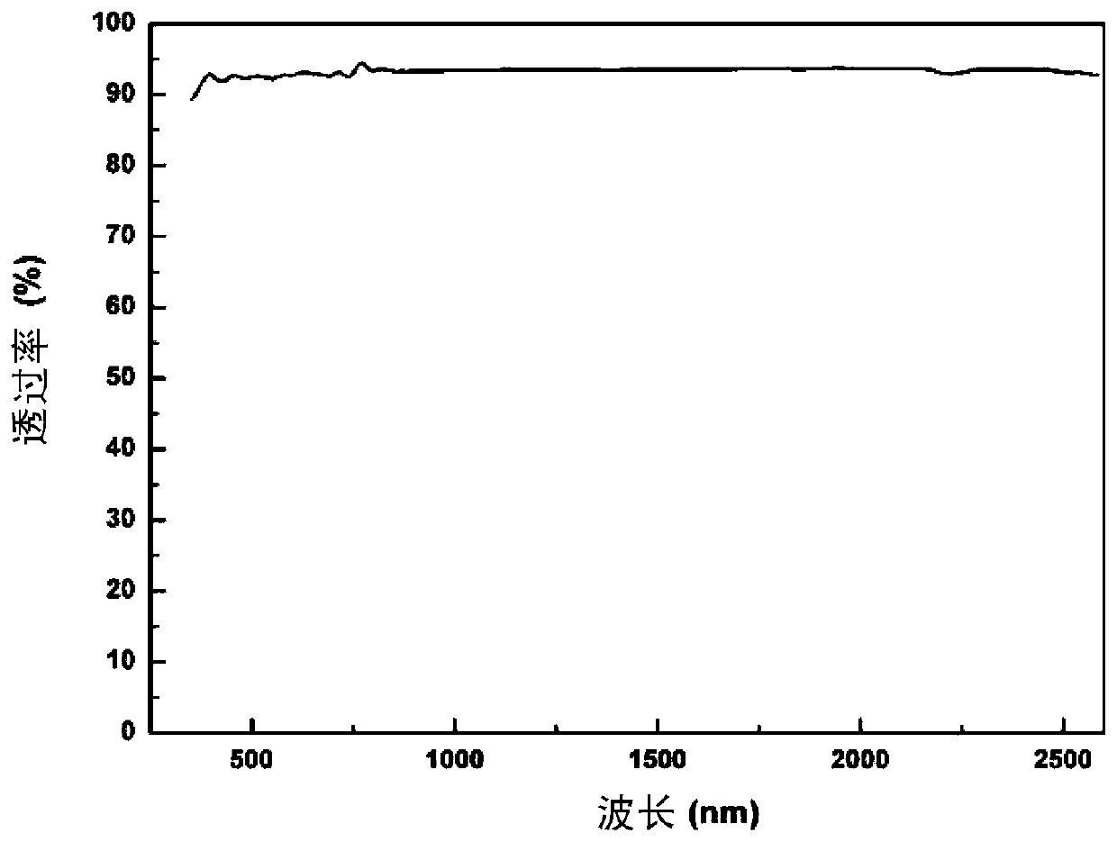
[0058] Form an aluminum-lithium alloy solid-state ion-conducting layer film on a nickel oxide film: prepare a transparent aluminum-lithium alloy film by magnetron reactive sputtering, put the substrate into a magnetron sputtering chamber, and select an aluminum-lithium target material AlLi (ratio 1:1), the sputtering power supply adopts DC power supply, and the power density is 1.5w / cm 2 , the atmosphere is pure argon, the pressure is 2.5Pa, and the room temperature is sputtered for 20 minutes to obtain an aluminum-lithium alloy thin film with a smooth surface, the thickness of which is 30nm, and the surface resistance is measured. The surface resistance is not less than 100kΩ. image 3 The transmission spectrum of the obtained solid ion-conducting layer film is shown. It can be seen that the visible light transmittance of the solid ion-conducting layer can reach more than 90%, and can be used in building smart windows, automobile rearview mirrors, and the like.
PUM
| Property | Measurement | Unit |
|---|---|---|
| thickness | aaaaa | aaaaa |
| thickness | aaaaa | aaaaa |
| thickness | aaaaa | aaaaa |
Abstract
Description
Claims
Application Information


