Semiconductor device
A technology for semiconductors and equipment, applied in the field of semiconductor equipment, can solve the problems of deterioration of retention characteristics and reduced yield, and achieve the effect of reducing power consumption
- Summary
- Abstract
- Description
- Claims
- Application Information
AI Technical Summary
Problems solved by technology
Method used
Image

Examples
no. 1 example
[0034]
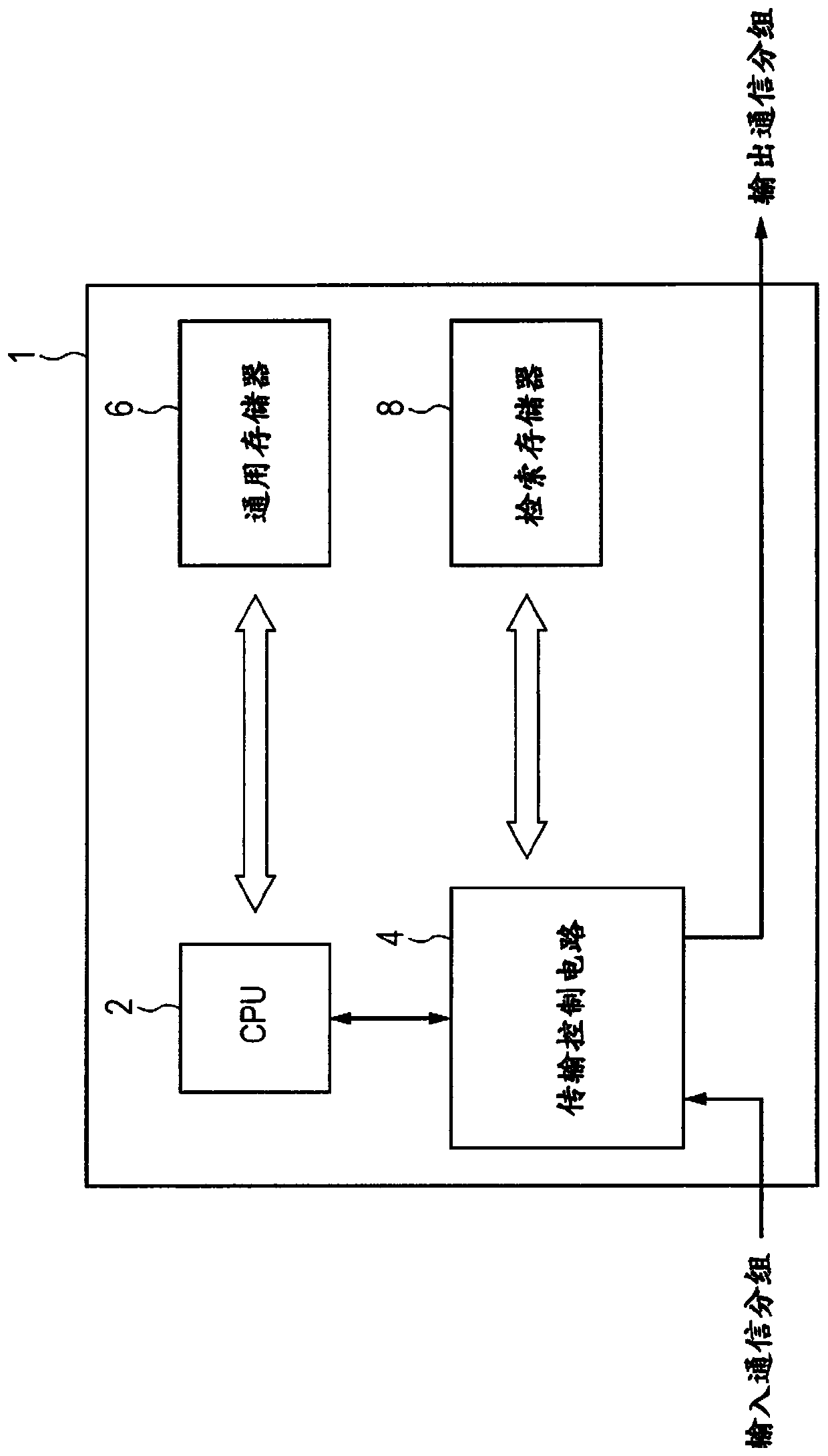
[0035] figure 1 is a diagram showing the configuration of the communication device 1 based on the first embodiment.
[0036] like figure 1 As shown, the communication device 1 is a communication device such as a switch or a router.
[0037] The communication device 1 includes a CPU (Central Processing Unit) 2 , a transmission control circuit 4 , a general-purpose memory 6 and a retrieval memory 8 .
[0038] CPU 2 controls the entire device.
[0039] The CPU 2 realizes various functions in cooperation with programs stored in the general-purpose memory 6 . For example, the general-purpose memory 6 may be configured with DRAM (Dynamic Random Access Memory) to establish an operating system (OS) in cooperation with the CPU 2 . The CPU 2 maintains and manages information necessary for transmission processing by exchanging information with adjacent communication devices and the like.
[0040] The transmission control circuit 4 executes transmission processing of com...
no. 2 example
[0115] Figure 7 is a diagram showing the configuration of a matching amplifier module based on the second embodiment.
[0116] like Figure 7 As shown, matching amplifiers are provided for each entry.
[0117] This example shows a case where a plurality of matched amplifiers (MA#0 to MA#(N−1)) are provided corresponding to each of a plurality of entries (entry 0 to entry (N−1)).
[0118] All matching amplifiers (MA#0 to MA#(N-1)) have the same configuration. Note that the matched amplifiers (MA#0 to MA#(N−1)) are also collectively referred to as matched amplifier MA#.
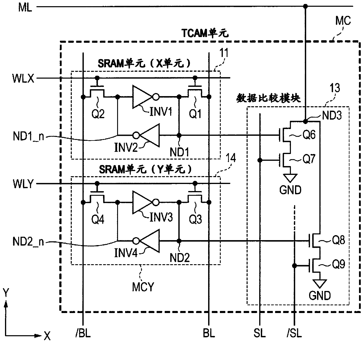
[0119] Similar to the first embodiment, each entry includes 40 memory cells MC and dummy memory cells DMC. The dummy memory cell DMC stores information on the retention characteristics of the potential of the corresponding match line ML.
[0120] The matching amplifier MA# includes an amplifier AP for amplifying data of the match line ML, a P-channel MOS transistor PT1 as a precharge circuit, a match-line...
no. 3 example
[0141] In recent years, the demand for a high-capacity retrieval system is increasing, and the layout area of the retrieval memory 8 is also increasing.
[0142] Figure 9 is a diagram showing a plurality of sections included in the retrieval memory 8 based on the third embodiment.
[0143] like Figure 9 As shown, this example shows an array configuration of 320 bits x 4k entries.
[0144] N blocks are provided.
[0145] Each of the blocks (0 to N-1) is provided with 8 sectors 12, each of the 8 sectors 12 has 40 bits x 128 entries.
[0146] In the third embodiment, information for selectively activating the match line holding circuit 50 is stored in the register 70 . The register 70 includes a plurality of storage modules 71 . The storage module 71 stores information to determine whether the match line hold circuit 50 is to be activated for each block.
[0147] In other words, when information is stored in the storage module 71 with respect to the block (block 0), all...
PUM
 Abstract
Description
Claims
Application Information