Manufacturing method of extra-high voltage VDMOS field effect transistor
A technology of field effect transistors and manufacturing methods, which is applied in the field of semiconductor power devices, can solve problems such as unsuitable VDMOS, slip lines, and increased number of particle defects, so as to save the N-epitaxy growth process and reduce production costs.
- Summary
- Abstract
- Description
- Claims
- Application Information
AI Technical Summary
Problems solved by technology
Method used
Image
Examples
Embodiment Construction
[0018] Below in conjunction with accompanying drawing and embodiment the present invention is further described:
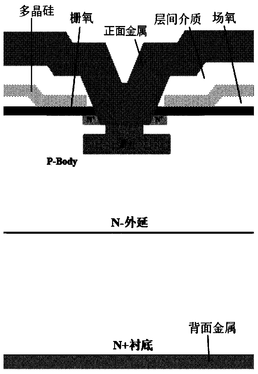
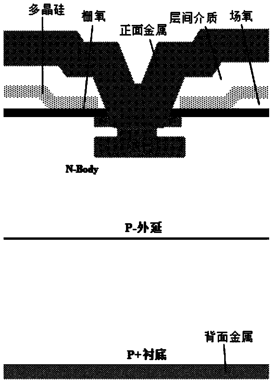
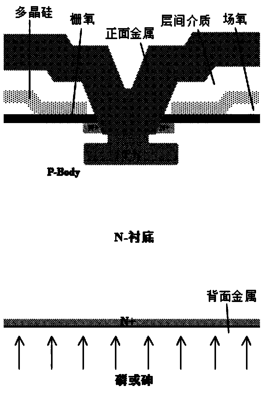
[0019] As shown in the figure, the manufacturing method of the UHV VDMOS field effect transistor of the present invention is provided.
[0020] If N-type VDMOS is produced, the production steps are as follows: 1. Use N-substrate instead of N+ substrate, and oxidize the front and back sides of N-substrate. The resistivity of the N-substrate sheet is selected according to the withstand voltage requirements of the manufactured device. The selection of the resistivity is the same as the selection of N-epitaxy in the existing N-type VDMOS production process. The higher the withstand voltage of the device, the N- The higher the resistivity of the substrate sheet, the thicker the thickness of the N-substrate sheet, which is generally 400-800um, but not limited to this thickness. 2. On the front side of the N-substrate, make the front structure of the N-type VDMOS accord...
PUM
 Abstract
Description
Claims
Application Information


