3D NAND flash memory and preparation method

A flash memory and suppression layer technology, applied in the direction of electrical components, electrical solid devices, circuits, etc., can solve the breakdown of the dielectric layer between the adjacent gate layers, the threshold voltage shift of the gate layer, and the leakage of adjacent gate layers, etc. problems, to reduce the coupling effect, reduce leakage, and ensure stability

Active Publication Date: 2019-07-23
YANGTZE MEMORY TECH CO LTD
View PDF7 Cites 16 Cited by
  • Summary
  • Abstract
  • Description
  • Claims
  • Application Information

AI Technical Summary

Problems solved by technology

[0005] In view of the above-mentioned shortcomings of the prior art, the purpose of the present invention is to provide a 3D NAND flash memory and its preparation method, which are used to solve the problem that the 3D NAND flash memory in the prior art is easily caused by the reduction of the thickness of the inter-gate dielectric layer. Leakage between gate layers may even cause the bre

Method used


Image

  • 3D NAND flash memory and preparation method
  • 3D NAND flash memory and preparation method
  • 3D NAND flash memory and preparation method

Examples


Example Embodiment

[0102] Embodiment one

[0103] see figure 1 , the present embodiment also provides a method for preparing a 3D NAND flash memory, the method for preparing the 3D NAND flash memory includes the following steps:

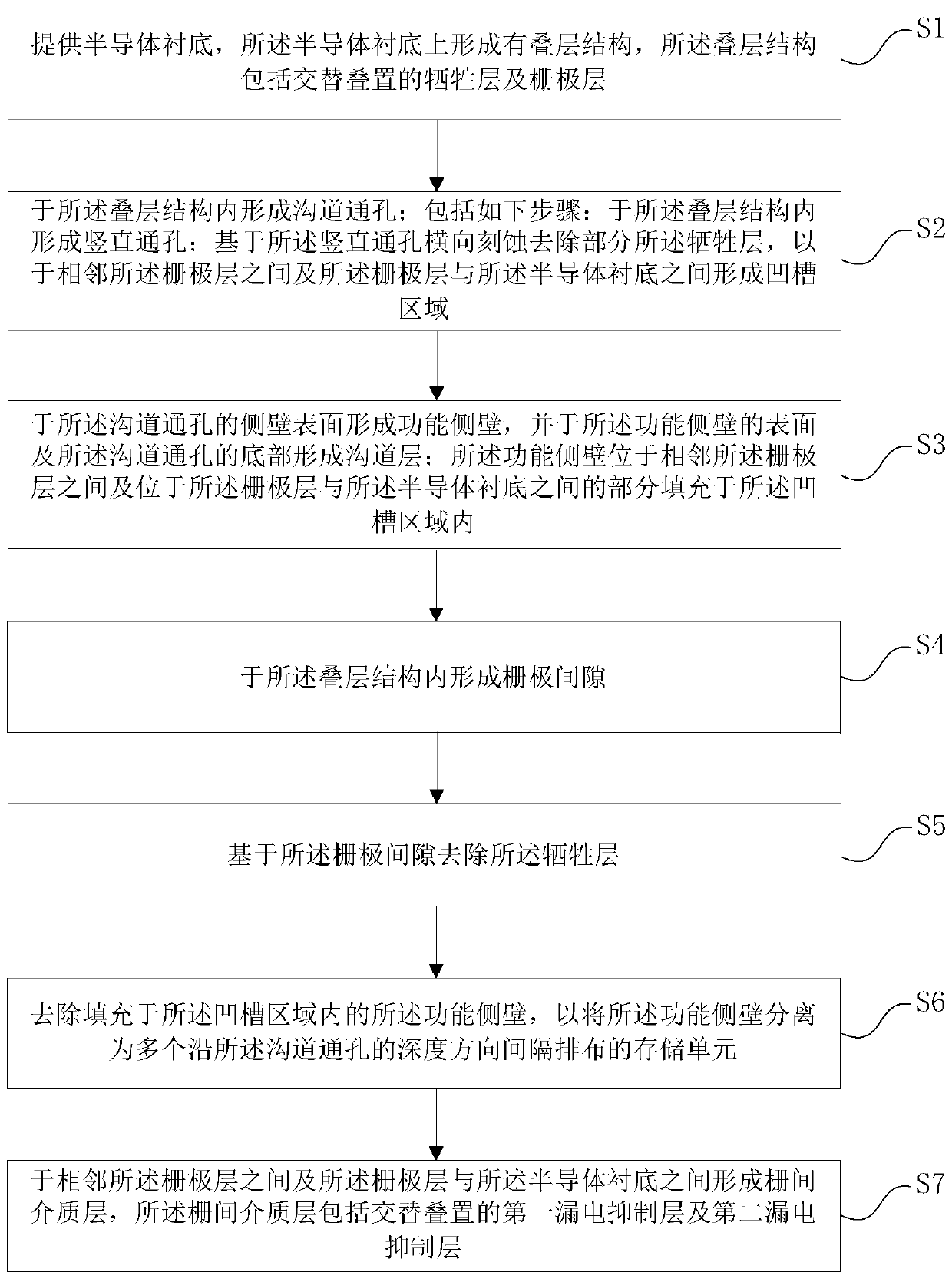
[0104] 1) providing a semiconductor substrate, on which a stacked structure is formed, and the stacked structure includes alternately stacked sacrificial layers and gate layers;

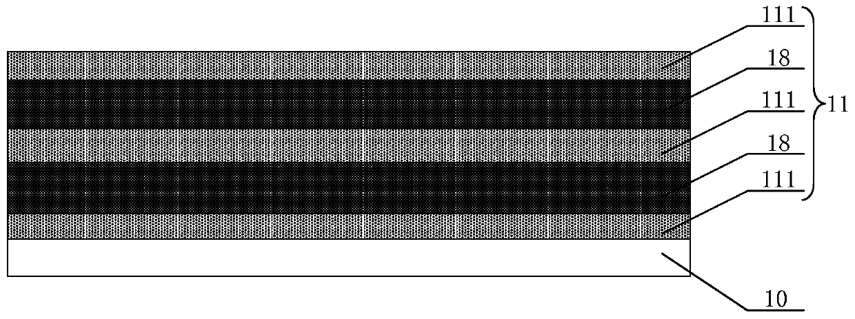
[0105] 2) Forming a channel via hole in the stacked structure; including the following steps: forming a vertical via hole in the stacked structure; laterally etching and removing part of the sacrificial layer based on the vertical via hole, to forming a groove region between adjacent gate layers and between the gate layer and the semiconductor substrate;

[0106] 3) forming a functional sidewall on the surface of the sidewall of the channel through hole, and forming a channel layer on the surface of the functional sidewall and the bottom of the channel through hole; The portion between the...

Example Embodiment

[0181] Embodiment two

[0182] read on Figure 24 and Figure 25 , this embodiment also provides a 3D NAND flash memory, the 3D NAND flash memory includes: a semiconductor substrate 10; a stacked structure 31, the stacked structure 31 is located on the semiconductor substrate 10, the stacked structure 31 includes alternately stacked first leakage suppression layers 171 and second leakage suppression layers 172; channel vias 12, the channel vias 12 are located in the stacked structure 31; functional sidewalls 13, the functional The sidewall 13 is located on the sidewall surface of the trench hole 12, and the functional sidewall 13 includes a plurality of storage units 132c separated and arranged at intervals along the depth direction of the trench hole 12, and the storage unit 132c is arranged in one-to-one correspondence with the gate layer 18; and a channel layer 14, the channel layer 14 is located in the channel via hole 12, and is located on the surface of the functional ...


PUM


Abstract

The invention provides a 3D NAND flash memory and a preparation method. The 3D NAND flash memory comprises a semiconductor substrate, a laminated structure, a channel through hole, a functional side wall and a channel layer, wherein the laminated structure is positioned on the semiconductor substrate, the laminated structure comprises inter-gate dielectric layers and grid layers which are superposed alternately; each inter-gate dielectric layer comprises first leakage inhibition layers and second leakage inhibition layers which are superposed alternately; the channel through hole is positionedinside the laminated structure; the functional side wall is positioned on the side wall surface of the channel through, the functional side wall comprises a plurality of separated storage units arranged along the depth direction of the channel through hole at intervals, and the storage units and the grid layers are arranged in a one-to-one correspondence mode; the channel layer is positioned inside the channel through hole, and is positioned on the surface of the functional side wall and the bottom of the channel through hole. According to the 3D NAND flash memory and the preparation method,electric leakage between adjacent grid layers can be reduced effectively, the breakdown resistance of the inter-gate dielectric layers between the adjacent grid layers is improved, and the coupling effect between the adjacent grid layers is reduced.

Description

technical field [0001] The invention belongs to the technical field of integrated circuit design and manufacture, and in particular relates to a 3D NAND flash memory and a preparation method. Background technique [0002] In recent years, the development of flash memory (Flash Memory) has been particularly rapid. The main feature of flash memory is that it can keep stored information for a long time without power on, and it has high integration, fast access speed, easy erasing and resetting. It has the advantages of writing and so on, so it has been widely used in many fields such as microcomputer and automatic control. In order to further increase the bit density (Bit Density) of the flash memory while reducing the bit cost (Bit Cost), three-dimensional flash memory (3D NAND) technology has been developed rapidly. [0003] The stack structure of the existing 3D NAND flash memory is formed by alternately stacking multiple gate layers (ie gate word line layers) and inter-gat...

Claims


Application Information

Patent Timeline
IPC IPC(8): H01L27/11551H01L27/11578
CPCH10B41/20H10B43/20
Inventor 肖莉红
Owner YANGTZE MEMORY TECH CO LTD
Why Eureka
Try Eureka