OLED device and preparation method thereof

A device and auxiliary cathode technology, which is applied in the field of OLED devices and its preparation, can solve problems such as voltage drop, and achieve the effect of improving voltage drop and increasing conductivity

Active Publication Date: 2019-07-23
SHENZHEN CHINA STAR OPTOELECTRONICS SEMICON DISPLAY TECH CO LTD
View PDF9 Cites 10 Cited by
  • Summary
  • Abstract
  • Description
  • Claims
  • Application Information

AI Technical Summary

Problems solved by technology

The driving voltage difference between the inner edge of the screen near the electrode interface area and the center area of ​​the screen is too large, and there is a problem of voltage drop (IR drop)
Therefore, it is necessary to find a new type of OLED device to solve the problem of voltage drop in the current OLED device.

Method used


Image

  • OLED device and preparation method thereof
  • OLED device and preparation method thereof
  • OLED device and preparation method thereof

Examples


Embodiment 1

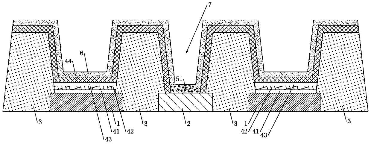
[0036] Such asfigure 1 As shown, the OLED device of this embodiment includes: a substrate (not shown in the figure), two anodes 1 , auxiliary cathodes 2 , two banks 3 , functional layers, thin film layers and surface cathodes 6 .

[0037] Wherein the two anodes 1 are arranged separately on the substrate, specifically, transparent electrodes made of transparent conductive films such as indium tin oxide (ITO) and indium zinc oxide (IZO) can be used, which have light transmission.

[0038] Wherein the auxiliary cathode 2 is arranged on the substrate between the two anodes 1, and the two dams 3 are relatively arranged above the two sides of the auxiliary cathode 2; the two dams 3 and the auxiliary cathode 2 A contact hole 7 is formed on the surface. Through the structure of the contact hole 7, the auxiliary cathode 2 and the surface cathode 6 are connected. Since the auxiliary cathode 2 has a small resistance, the voltage drop problem can be effectively solved by conducting the au...

Embodiment 2

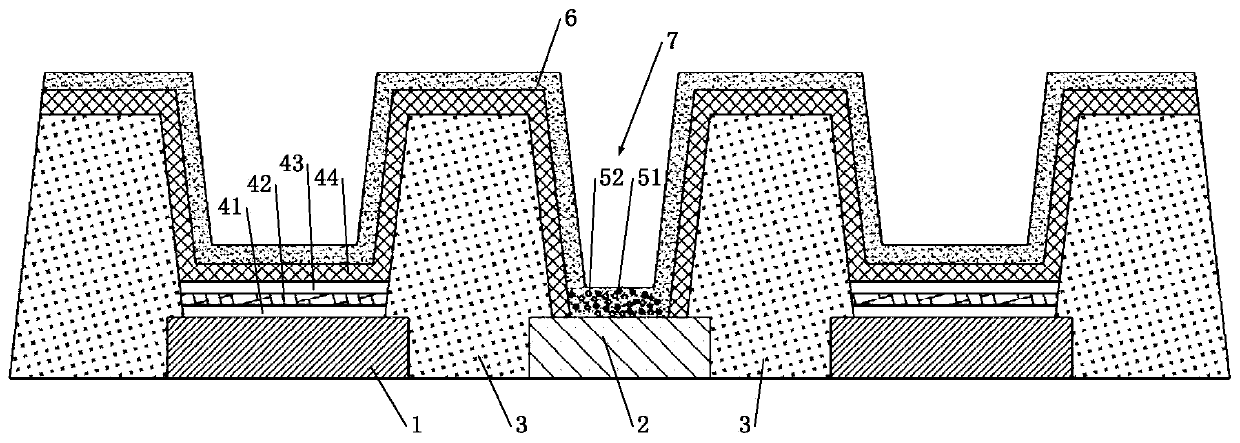
[0045] In the following, only the differences between the present embodiment and the first embodiment will be described, and the similarities will not be repeated here.

[0046] Such as figure 2 As shown, a conductive material 52 is also added in the thin film layer. Wherein the good conductor material is graphene and / or nano silver. The external conductor material 52 can enhance the conductivity of the thin film layer, thereby effectively solving the problem of voltage drop.

Embodiment 3

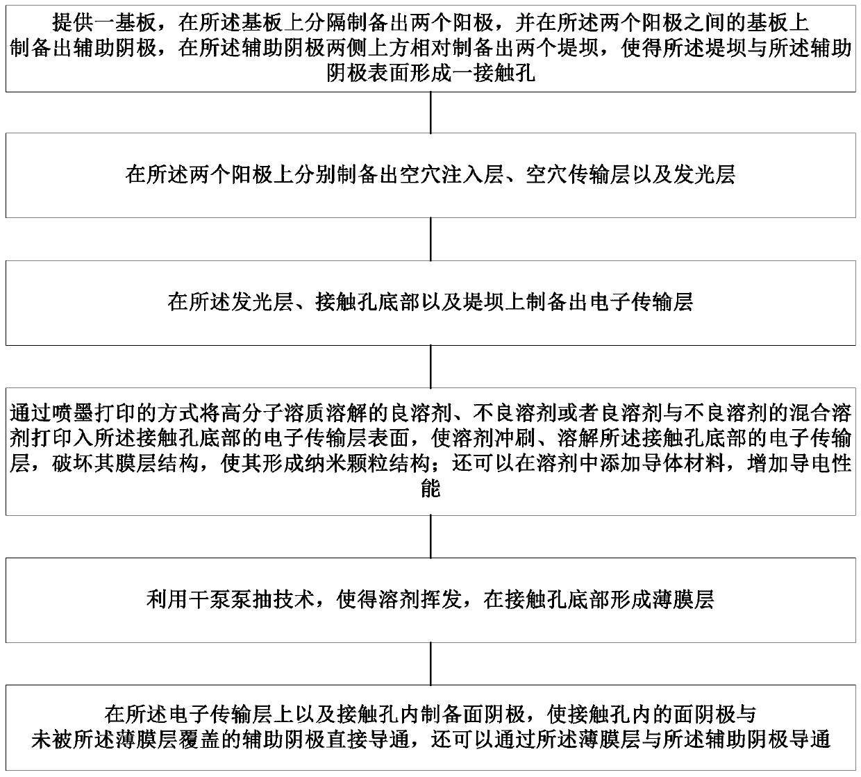
[0048] Such as image 3 As shown, this embodiment provides a method for preparing an OLED device. It includes: S1, providing a substrate, preparing two anodes 1 separately on the substrate, and preparing an auxiliary cathode 2 on the substrate between the two anodes 1, above the two sides of the auxiliary cathode 2 Two dams 3 are relatively prepared, so that a contact hole 7 is formed between the dam 3 and the surface of the auxiliary cathode 2; S2, a hole injection layer 41 and a hole transport layer are respectively prepared on the two anodes 1 42 and the luminescent layer 43; S3, the electron transport layer 44 is prepared on the luminescent layer 43, the bottom of the contact hole 7 and the dam 3; S4, a good solvent, a poor solvent or a good solvent for dissolving the polymer solute by inkjet printing A mixed solvent of a good solvent and a poor solvent is printed into the surface of the electron transport layer 44 at the bottom of the contact hole 7, so that the solvent ...


PUM


Abstract

The invention relates to an OLED device and a preparation method thereof. The OLED device comprises a substrate, two anodes, an auxiliary cathode, two dams, a functional layer, a thin film layer and asurface cathode. A good solvent and a poor solvent dissolved by a macromolecular solute or a mixed solvent of the good solvent and the poor solvent are printed into an electron transport layer at thebottom of a contact hole through ink-jet printing, so that the solvent scours and dissolves the electron transport layer at the bottom of the contact hole, a film layer structure of the electron transport layer is damaged to form a nanoparticle structure, and then the solvent is removed to form the thin film layer. Due to the agglomeration effect of the nanoparticles, the uniformity of the thin film layer is reduced, so that the surface cathode can be directly conducted with the auxiliary cathode which is not covered by the thin film layer, and the problem of voltage drop is solved; and in addition, a conductor material can be added into a solvent for washing the electron transport layer, so that the conductivity of the thin film layer is improved, the surface cathode can be conducted with the auxiliary cathode through the thin film layer mixed with the conductor material, and the problem of voltage drop is further solved.

Description

technical field [0001] The invention relates to the field of display technology, in particular to an OLED device and a preparation method thereof. Background technique [0002] OLED (full name in English: Organic Light-Emitting Diode, referred to as OLED) devices are also called organic electro-laser display devices and organic light-emitting semiconductors. The basic structure of an OLED is a thin, transparent indium tin oxide (ITO) with semiconducting properties connected to the positive electrode of electricity, plus another metal surface cathode, wrapped into a sandwich structure. The whole structural layer includes: hole transport layer (HTL), light emitting layer (EL) and electron transport layer (ETL). When the power is supplied to an appropriate voltage, positive holes and surface cathode charges will combine in the light-emitting layer, and under the action of Coulomb force, they will recombine with a certain probability to form excitons (electron-hole pairs) in an...

Claims


Application Information

Patent Timeline
Patent Type & Authority Applications(China)
IPC IPC(8): H01L51/52H01L51/50H01L51/56
CPCH10K50/16H10K50/824H10K71/00
Inventor 潘凌翔刘明
Owner SHENZHEN CHINA STAR OPTOELECTRONICS SEMICON DISPLAY TECH CO LTD
Why Eureka
Try Eureka