Optical modulation terahertz broadband wave absorber based on doped silicon

A wave absorber and light modulation technology, applied in the field of terahertz wave absorption, can solve the problems of difficult processing, narrow absorption bandwidth, low absorption rate, etc., and achieve the effects of simple structure, wide absorption bandwidth and high absorption rate

Pending Publication Date: 2019-07-23
CHINA JILIANG UNIV
View PDF3 Cites 17 Cited by
  • Summary
  • Abstract
  • Description
  • Claims
  • Application Information

AI Technical Summary

Problems solved by technology

[0004] In order to overcome the complex structure, difficult processing, low absorption rate and narrow absorption bandwidth of existing wave absorbers, the present invention provides a light-modulated terahertz broadband wave absorber based on doped silicon to solve the ...

Method used


Image

  • Optical modulation terahertz broadband wave absorber based on doped silicon
  • Optical modulation terahertz broadband wave absorber based on doped silicon
  • Optical modulation terahertz broadband wave absorber based on doped silicon

Examples


Embodiment 1

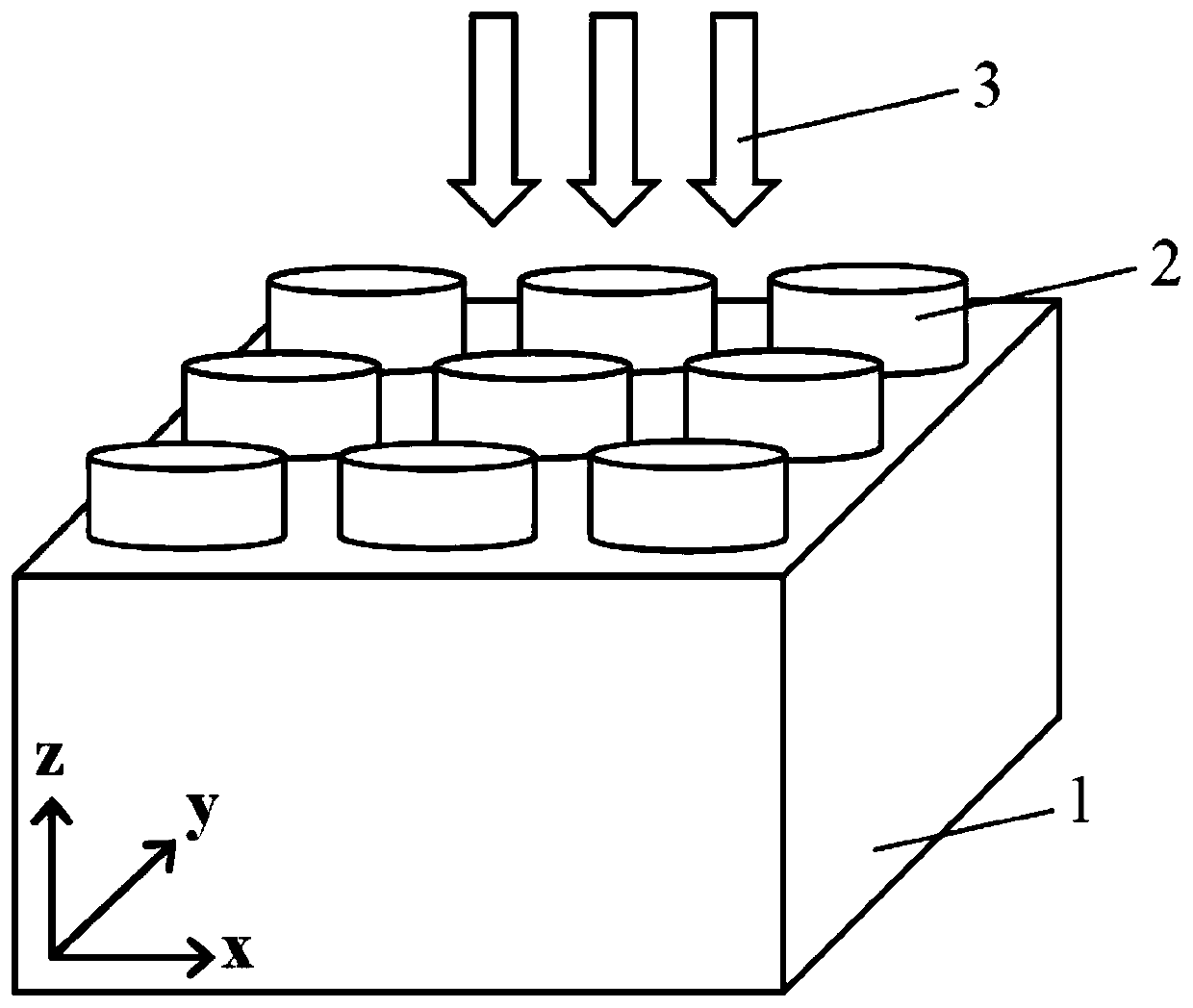
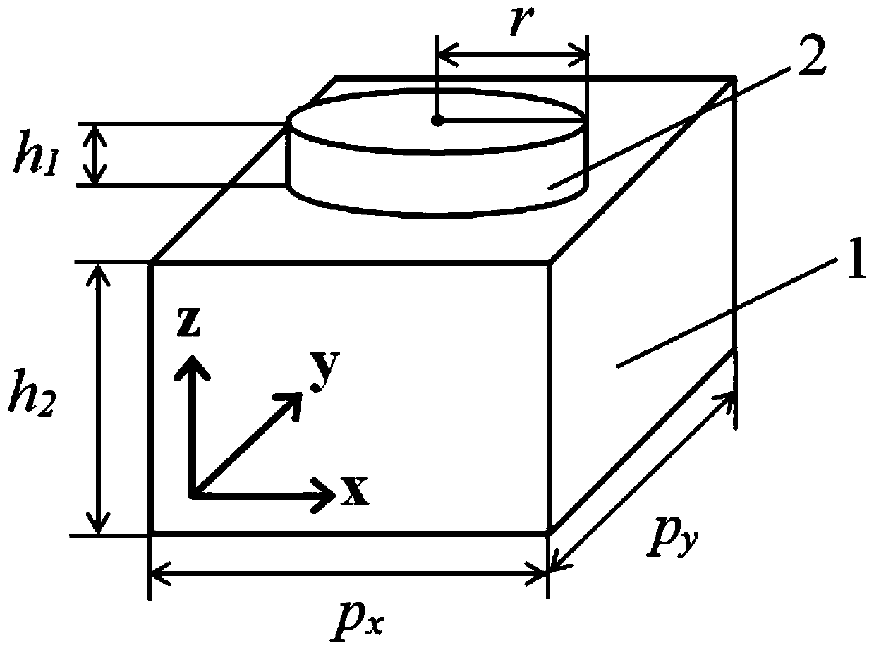
[0026] Embodiment 1: as attached figure 1 As shown, a light-modulated terahertz broadband absorber based on doped silicon includes a three-layer structure, from bottom to top: silicon substrate layer 1, metamaterial layer 2, and optical pump source 3; metamaterial layer 2 consists of a cylindrical Composed of structural arrays, it is periodic in the xoy plane, and the cylindrical structures are periodically arranged on the silicon substrate layer 1, as attached figure 2 As shown, it is a schematic diagram of the structure of this embodiment in one cycle. In this embodiment, the structural parameters of the cylindrical structure of the metamaterial layer 2 in one cycle are radius r=60 μm, height h 1 =40μm, the structural parameter of the silicon substrate layer 1 in one cycle is the cycle length p x =p y = 150μm, height h 2 =250 μm, the silicon substrate layer 1 and the metamaterial layer 2 of the wave absorber are made of boron-doped p-type silicon. The fabrication of the...

Embodiment 2

[0029] Embodiment 2: as attached Figure 6 As shown, a light-modulated terahertz broadband absorber based on doped silicon includes a three-layer structure, from bottom to top: silicon substrate layer 1, metamaterial layer 2, and optical pump source 3; metamaterial layer 2, composed of Composed of a square structure array, it is periodic in the xoy plane, and the square structure is periodically arranged on the silicon substrate layer 1, as shown in the attached Figure 7 As shown, it is a schematic diagram of the structure of this embodiment in one cycle. In this embodiment, the structural parameters of the square structure of the metamaterial layer 2 in one cycle are side length a=90 μm, height H 1 =40μm, the structural parameter of the silicon substrate layer 1 in one period is the period length P x =P y = 150μm, height H 2 =250 μm, the silicon substrate layer 1 and the metamaterial layer 2 of the wave absorber are made of boron-doped p-type silicon. The fabrication of ...


PUM


Abstract

The invention discloses an optical modulation terahertz broadband wave absorber based on doped silicon. A three-layer structure comprises a silicon substrate layer, a metamaterial layer and an opticalpumping source, which are sequentially arranged from bottom to top; the silicon substrate layer and the metamaterial layer are both boron-doped p-type silicon materials; and the metamaterial layer iscomposed of a unit structure array. The unit structure arrays are periodically arranged on the silicon substrate layer in an xoy plane; terahertz waves are incident on the wave absorber; the opticalpumping source is coupled into the wave absorber and excites electromagnetic resonance to realize broadband absorption of terahertz waves; and the optical pumping source generates a pumping light beamwhich is directly incident on the silicon substrate layer and the metamaterial layer to change the carrier concentration of doped silicon and realize the modulation function of the wave absorber on the absorption frequency band and the absorption rate of the terahertz waves. The terahertz wave absorption device is simple in structure, single in material, easy to process, high in terahertz wave absorption rate and wide in absorption bandwidth, has a light modulation function, and can be widely applied to multiple fields of imaging, stealth, communication, terahertz detection and the like.

Description

technical field [0001] The invention relates to a light modulation terahertz broadband absorber based on doped silicon, belonging to the technical field of terahertz wave absorbing. Background technique [0002] With the development of society and the maturity of technology, absorbers are more and more widely used in imaging, light detection, wireless communication, military stealth, biological sensing and other fields. [0003] On August 23, 2018, Nanjing University of Posts and Telecommunications proposed "a polarization-insensitive ultra-broadband terahertz absorber with a multi-layer structure" with the application number 201810965018.3, including the bottom reflector and the tailored Dielectric substrate, the first resonant unit composed of one layer of metal patches is arranged on the top of the dielectric substrate, and the second resonant unit composed of two layers of metal patches is embedded inside the dielectric substrate. The invention adopts multi-layer structu...

Claims


Application Information

Patent Timeline
IPC IPC(8): H01Q17/00H01Q15/00G02B5/00
CPCH01Q17/007H01Q15/0086G02B5/003
Inventor 郎婷婷沈婷婷胡杰
Owner CHINA JILIANG UNIV
Why Eureka
Try Eureka