Method for preparing three-dimensional atom probe sample in rotary mode

An atom probe, rotary technology, applied in the field of micro-nano-scale material sample preparation, can solve the problems of missing sample area, difficult to ensure that the needle tip sample contains the interface of interest, and lack of expected data, etc., to improve the experimental efficiency. Effect

Active Publication Date: 2019-08-02
NANJING UNIV OF SCI & TECH
View PDF6 Cites 8 Cited by
  • Summary
  • Abstract
  • Description
  • Claims
  • Application Information

AI Technical Summary

Problems solved by technology

[0004] The commonly used method for preparing needle-tip samples with focused ion beams is to place the sampling interface vertically on a needle tip. For samples whose interface growth direction is perpendicular to the upper surface of the planar bulk material, the tissue structure on both sides of the interface will The difference of the ion beam leads to the inconsistency of the etching speed on both sides of

Method used


Image

  • Method for preparing three-dimensional atom probe sample in rotary mode
  • Method for preparing three-dimensional atom probe sample in rotary mode
  • Method for preparing three-dimensional atom probe sample in rotary mode

Examples


Embodiment 1

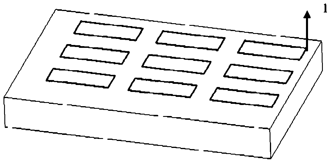
[0054] By using the cross-cut fin structure sample in the fin field effect transistor of the present invention, the three-dimensional atom probe tip sample can be prepared for the fin structure of the fin field effect transistor. This method is different from the traditional method of vertically placing the entire fin structure on a needle tip, but adopts the method of rotating 90° counterclockwise. The fin structure in the semiconductor device is placed perpendicular to the growth direction. The schematic diagram of the present invention is as follows figure 1 shown. Then use the focused ion beam to cut the triangular prism-like strip sample into several small pieces, that is, only a small section of the fin structure is included in each 3D atom probe tip sample, and then cut multiple tip samples for 3D atom probe Technical characterization.

[0055] The following takes the processing of the three-dimensional atom probe tip sample of the fin field effect transistor as an exa...

Embodiment 2

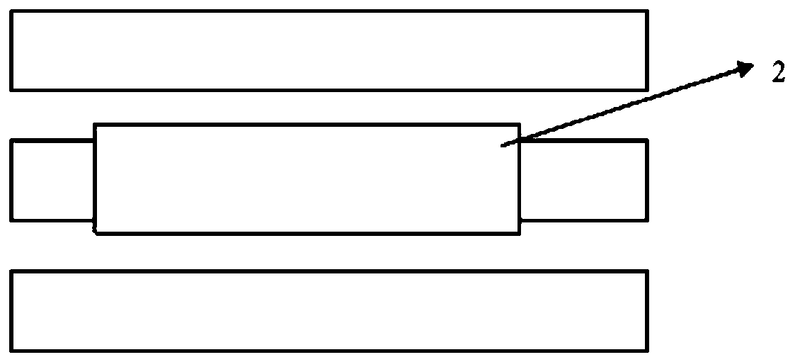
[0078] The invention is also applicable to samples with a layered structure, and can perform three-dimensional atom probe sample preparation on the interface between layers. The sample in this example is a layered alloy formed by a layer of Cr structure and a layer of ZrNiSn structure and the interface formed by the mutual diffusion of the two, as shown in Figure 12(a). The preparation method of the needle tip sample is the same as in Example 1, and the triangular prism-like strip sample is extracted at the interface, as shown in Figure 12(b), and then rotated 90° counterclockwise so that the upper right-angled surface 15 of the strip sample is horizontally upward, while The smooth upper surface 13 of the planar bulk material is perpendicular to the platform surface of the silicon base, so that the slope 14 trimmed on the lower side of the long sample can contact the silicon base, and Pt is deposited on the contact. Such as Figure 13 The interface and sampling points are sho...


PUM

PropertyMeasurementUnit
Thicknessaaaaaaaaaa

Abstract

The invention belongs to the field of material preparation, and particularly relates to a method for preparing a three-dimensional atom probe sample in a rotary mode. The method comprises the following steps: Step 1: placing a planar block material on a sample table, and depositing a Pt layer on the upper surface of the planar block material along the region of interest; Step 2: extracting a triangular prism-like long strip sample: separating the region of interest from a substrate by using a focused ion beam; Step 3: rotating triangular prism-like long strip sample: transferring the triangular prism-like long strip sample extracted in Step 2 to a rotating needle point, rotating the rotating needle point, and transferring the rotated triangular prism-like long strip sample to an in-situ nano operating rod; and Step 4: shaping Shaping a needle point sample. According to the invention, after the triangular prism-like long strip sample is rotated by 90 degrees by an instrument, the needlepoint sample is further obtained, and after laser excitation, the obtained three-dimensional atom probe data can be reconstructed by software to obtain the data of an interface and tissue structureson two sides of the interface, so that the element distribution and structure in the needle point sample can be analyzed accurately.

Description

technical field [0001] The invention belongs to the field of micro-nano-scale material sample preparation, in particular to a method for preparing a three-dimensional atom probe sample in a rotating manner. Background technique [0002] The 3D atom probe is a measurement and analysis method with atomic-level spatial resolution. Based on the principle of "field evaporation", the 3D atom probe applies a strong voltage pulse or laser pulse to the sample, turning its surface atoms into ions one by one, removes and collects them, and finally obtains a complete needle tip sample through software reconstruction. The three-dimensional atom probe has a significant effect on the analysis of element segregation, dislocation composition, precipitated phase composition and interface composition in materials. The use of three-dimensional atom probe technology to study the distribution of trace elements in materials is a new method for characterizing metals and semiconductors in recent ye...

Claims


Application Information

Patent Timeline
IPC IPC(8): G01Q30/20G01Q60/38
CPCG01Q30/20G01Q60/38
Inventor 胡蓉陈琪吴杏苹沙刚
Owner NANJING UNIV OF SCI & TECH
Why Eureka
Try Eureka