Method for growing LED epitaxial structure

A technology of epitaxial structure and growth method, which is applied to electrical components, circuits, semiconductor devices, etc., can solve the problems of reducing the anti-aging ability and anti-static ability of LED devices, reducing the optical output power of LED devices, and increasing leakage channels of LED devices. Achieve the effect of improving lattice mismatch, protecting crystal ordering, and improving bottom warpage

Inactive Publication Date: 2019-08-06
XIANGNENG HUALEI OPTOELECTRONICS
View PDF4 Cites 1 Cited by
  • Summary
  • Abstract
  • Description
  • Claims
  • Application Information

AI Technical Summary

Problems solved by technology

Generally speaking, the dislocation density of GaN grown by MOCVD method is 1×10 10 ~3×10 10 piece / m 2 , Dislocation defects severely damage the original crystal order of gallium nitride, thereby reducing the light output power of LED devices. For example, screw dislocations extend from the bottom layer of the LED epitaxial structure to the surface of the LED epitaxial structure, and pass through the LED light-emitting layer. Screw dislocations lead to non-luminescent radiation of holes and electrons in the LED light-emitting layer, which reduces the light output power of the LED device
In addition, dislocation defects will also increase the leakage channels of LED devices, which will accelerate the aging of LED devices due to the increase in leakage channels. Dislocation defects will also increase the breakdown path of LED devices and cause LED antistatic capabilities to weaken
At present, the LED market requires low driving voltage for LED chips, especially under high current density, the smaller the driving voltage and the higher the light efficiency, the better, but the current density is too high. The ability to expand the current is limited, and it is very easy to cause damage to the LED device, which eventually leads to a decrease in the anti-aging ability and anti-static ability of the LED device

Method used


Image

  • Method for growing LED epitaxial structure
  • Method for growing LED epitaxial structure
  • Method for growing LED epitaxial structure

Examples


Embodiment 1

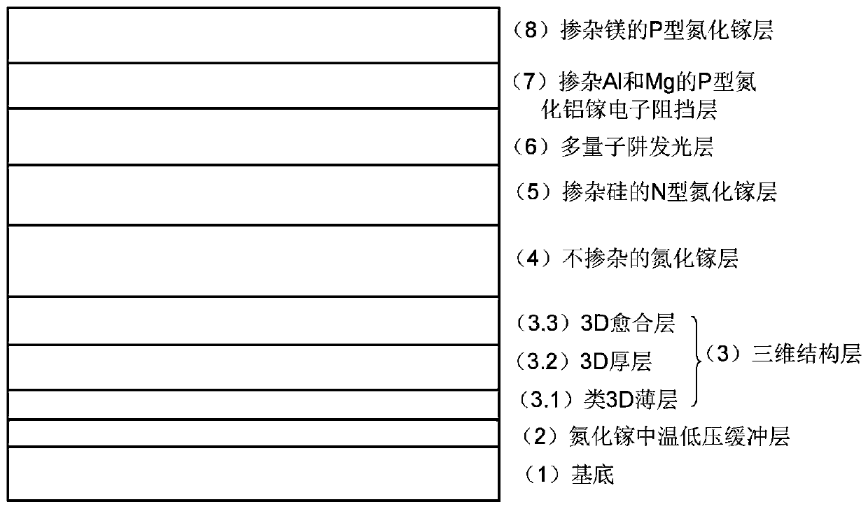
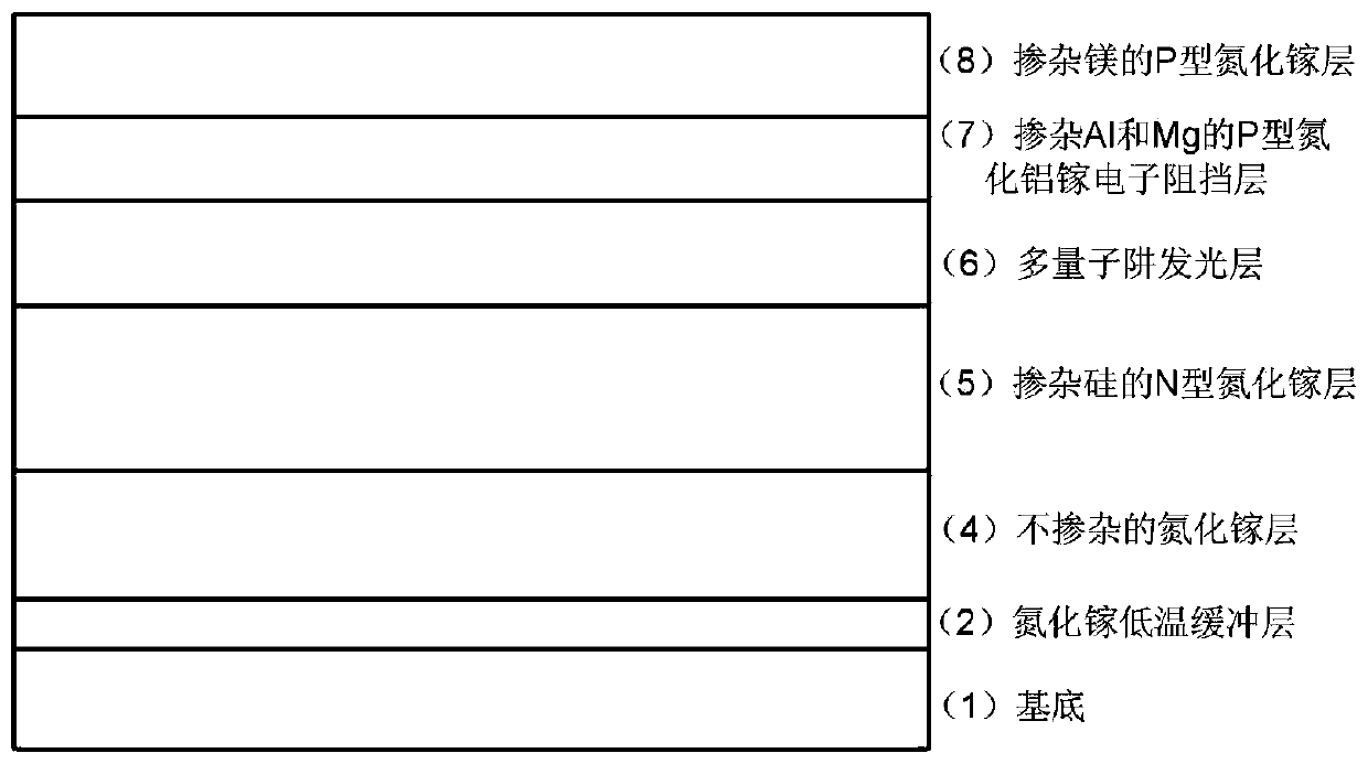
[0037] A method for growing an LED epitaxial structure, including the process of growing a gallium nitride medium-temperature and low-pressure buffer layer and a three-dimensional structure layer, specifically:

[0038] Step 2: growing GaN medium temperature and low pressure buffer layer;

[0039] Step 3: growing a three-dimensional structure layer;

[0040] The three-dimensional structural layer includes a 3D-like thin layer, a 3D thick layer and a 3D healing layer grown sequentially from bottom to top.

[0041] The step 2 is specifically: control the temperature of the reaction chamber at 800° C., the pressure at 100 mbar, feed ammonia gas with a flow rate of 35 L / min and trimethylgallium with a flow rate of 65 sccm, and grow a thickness of 20nm gallium nitride medium temperature and low pressure buffer layer.

[0042] The step 3: growing a three-dimensional structure layer includes the following steps:

[0043] Step 3.1: grow a 3D-like thin layer, specifically, control t...


PUM

PropertyMeasurementUnit
thicknessaaaaaaaaaa

Abstract

The invention provides a method for growing an LED epitaxial structure, which includes the process of growing a GaN medium-temperature low-pressure buffer layer and a three-dimensional structure layer. The method specifically includes the following steps: S2, growing a GaN medium-temperature low-pressure buffer layer; and S3, growing a three-dimensional structure layer. The three-dimensional structure layer includes a 3D-like thin layer, a 3D thick layer and a 3D healing layer grown in turn from bottom to top. The step S3 of growing a three-dimensional structure layer includes the following sub-steps: S3.1, growing a 3D-like thin layer; S3.2, growing a 3D thick layer, which is a silicon-doped GaN layer; and S3.3, growing a 3D healing layer. The lattice mismatch can be improved, the dislocation defect can be reduced, and the light output power, anti-aging ability and anti-static ability of LED devices can be improved.

Description

technical field [0001] The invention relates to the technical field of LEDs, in particular to a method for growing an LED epitaxial structure. Background technique [0002] In the process of growing LED epitaxial structures on the substrate by using the metal chemical vapor deposition method MOCVD in the traditional LED epitaxial structure growth method, point dislocations, ductile dislocations and helical dislocations often occur due to the lattice mismatch between the substrate and GaN. Growth defects of dislocations. Generally speaking, the dislocation density of GaN grown by MOCVD method is 1×10 10 ~3×10 10 piece / m 2 , Dislocation defects severely damage the original crystal order of gallium nitride, thereby reducing the light output power of LED devices. For example, screw dislocations extend from the bottom layer of the LED epitaxial structure to the surface of the LED epitaxial structure, and pass through the LED light-emitting layer. Screw dislocations lead to no...

Claims


Application Information

Patent Timeline
Patent Type & Authority Applications(China)
IPC IPC(8): H01L33/00H01L33/06H01L33/12H01L33/32
CPCH01L33/0066H01L33/0075H01L33/06H01L33/12H01L33/325
Inventor 林传强
Owner XIANGNENG HUALEI OPTOELECTRONICS
Why Eureka
Try Eureka