Preparation method of MWT solar cell
A technology for solar cells and cells, applied in circuits, photovoltaic power generation, electrical components, etc., can solve problems such as increased fragmentation rate, achieve the effects of reducing fragmentation rate, improving battery conversion efficiency, and reducing warpage
- Summary
- Abstract
- Description
- Claims
- Application Information
AI Technical Summary
Problems solved by technology
Method used
Image
Examples
preparation example Construction
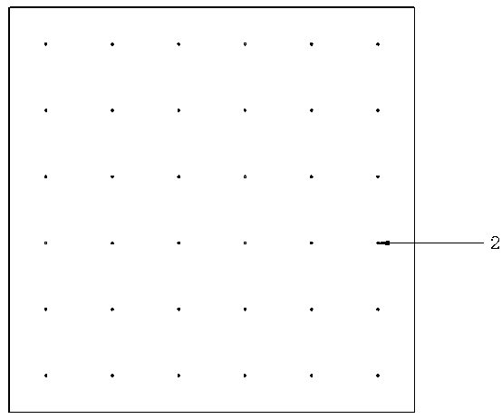
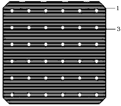
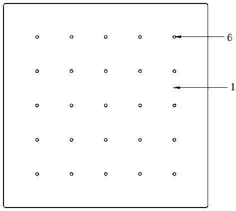
[0041] like Figure 1 to Figure 5 As shown, the technical solution provided by the present invention is a preparation method of a MWT solar cell, and the preparation method comprises the following steps:
[0042] Step 1, using a thin silicon wafer 1 as the substrate of the battery, removing the damaged layer on the surface of the silicon wafer 1, cleaning and texturing the silicon wafer 1, reducing the recombination rate of photogenerated carriers, and simultaneously Made of suede to reduce reflectivity;
[0043] Step 2, Diffusion: Deposit dopant sources on the substrate of silicon wafer 1 and perform diffusion to prepare a PN junction. Silicon wafer 1 is diffused on one side in a diffusion furnace in a back-to-back manner;
[0044] Step 3, etching: removing the PN junction around and on the back of the diffused silicon wafer 1, removing the phosphosilicate glass, and performing back polishing;
[0045] Step 4, annealing: annealing the silicon wafer 1 after etching;
[0046...
Embodiment 1
[0057] 1. Silicon wafer 1: use solar-grade P-type monocrystalline or polycrystalline silicon wafer 1 with a thickness of 140 μm as the substrate;
[0058] 2. Laser drilling 2: Press the silicon wafer 1 as figure 1 As shown in the 6×6 array pattern, use the laser to make 2 holes corresponding to the laser holes on the cell.
[0059] 3. Texturing: Cleaning and texturing using conventional chemical cleaning and texturing methods;
[0060]4. Diffusion: Use POCl3 diffusion source for high-temperature back-to-back single-sided diffusion, and the diffusion resistance is controlled at 30-150Ω;
[0061] 5. Etching: Use conventional chemical solutions for chemical post-cleaning, remove the peripheral and back PN junctions, remove the phosphosilicate glass formed on the surface of the silicon substrate after diffusion, and perform back polishing;
[0062] 6. Annealing: the etched silicon wafer 1 is annealed at a temperature of 600-750° C. using a conventional atmospheric pressure diffu...
Embodiment 2
[0073] 1. Silicon wafer 1: use solar-grade P-type monocrystalline or polycrystalline silicon wafer 1 with a thickness of 140 μm as the substrate;
[0074] 2. Texturing: Cleaning and texturing using conventional chemical cleaning and texturing methods;
[0075] 3. Diffusion: use POCl3 diffusion source for high-temperature back-to-back single-sided diffusion, and the diffusion resistance is controlled at 30-150Ω;
[0076] 4. Etching: Use conventional chemical solutions for chemical post-cleaning, remove the peripheral and back PN junctions, remove the phosphosilicate glass formed on the surface of the silicon substrate after diffusion, and perform back polishing;
[0077] 5. Annealing: the etched silicon wafer 1 is annealed at a temperature of 600-750° C. in a conventional atmospheric pressure diffusion furnace.
[0078] 6. Preparation of the passivation layer on the back: use chemical vapor deposition (CVD) to coat a layer of AlOx passivation film with a thickness of 5-50nm on...
PUM
| Property | Measurement | Unit |
|---|---|---|
| thickness | aaaaa | aaaaa |
| thickness | aaaaa | aaaaa |
| refractive index | aaaaa | aaaaa |
Abstract
Description
Claims
Application Information


