
Optical proximity correction method, mask manufacturing method and graphical process

An optical proximity correction and mask technology, which is applied in the photoengraving process of the pattern surface, optics, and originals for optomechanical processing, etc., can solve the problems of low graphics resolution and achieve the effect of improving the resolution

Active Publication Date: 2019-08-13
SEMICON MFG INT (SHANGHAI) CORP +1
View PDF10 Cites 0 Cited by
  • Summary
  • Abstract
  • Description
  • Claims
  • Application Information

AI Technical Summary

Problems solved by technology

[0005] However, the resolution of the optical proximity corrected pattern in the prior art is low

Method used


Image

  • Optical proximity correction method, mask manufacturing method and graphical process
  • Optical proximity correction method, mask manufacturing method and graphical process
  • Optical proximity correction method, mask manufacturing method and graphical process

Examples


Embodiment Construction

[0028] As mentioned in the background, the resolution of graphics obtained by optical proximity correction in the prior art is relatively low.

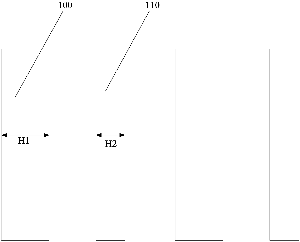
[0029] An optical proximity correction method, comprising: providing if figure 1 As shown in the target figure, the target figure includes a first figure 100 and a second figure 110, the first figure 100 and the second figure are staggered along the first direction, the first figure 100 and the second figure 110 are long strips, the first The width direction of the graphic 100 and the second graphic 110 is parallel to the first direction, the first graphic 100 has a first width H1, the second graphic has a second width H2, and the first width H1 is greater than the second width H2; OPC is performed on the target graphic The correction is to obtain a correction graph, where the correction graph includes a first correction graph corresponding to the first graph 100 and a second correction graph corresponding to the second graph 110 .

...


PUM

PropertyMeasurementUnit
widthaaaaaaaaaa

Abstract

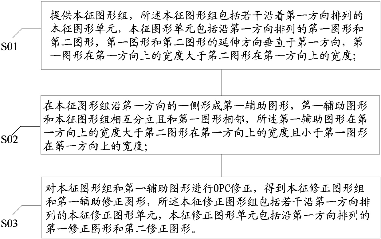
The invention discloses an optical proximity correction method, a mask manufacturing method and a graphical process. The optical proximity correction method comprises the steps of: forming a first auxiliary graph on one side of an intrinsic graph group in the first direction, wherein the first auxiliary graph and the intrinsic graph group are separated from each other and are adjacent to the firstgraph, and the width of the first auxiliary graph in the first direction is larger than that of the second graph in the first direction and smaller than that of the first graph in the first direction; carrying out OPC correction on the intrinsic graph group and the first auxiliary graph to obtain an intrinsic correction graph group and a first auxiliary correction graph, wherein the intrinsic correction graph group comprises a plurality of intrinsic correction graph units arranged in the first direction, and the intrinsic correction graph units comprise first correction graphs and second correction graphs which are arranged in the first direction. According to the method, the resolution of the second correction graphs is improved.

Description

technical field [0001] The invention relates to the field of semiconductor manufacturing, in particular to an optical proximity correction method, a mask plate manufacturing method and a patterning process. Background technique [0002] Photolithography technology is a crucial technology in semiconductor manufacturing technology. Photolithography technology can realize the transfer of graphics from the mask to the surface of the silicon wafer to form semiconductor products that meet the design requirements. The photolithography process includes an exposure step, a development step performed after the exposure step, and an etching step after the development step. In the exposure step, light is irradiated onto the silicon wafer coated with photoresist through the light-transmitting area of ​​the mask, and the photoresist reacts chemically under the irradiation of light; The photoresist is different to the degree of dissolution of the developer, forming a photoresist pattern, ...

Claims


Application Information

Patent Timeline
Patent Type & Authority Applications(China)
IPC IPC(8): G03F1/36
CPCG03F1/36
Inventor 杜杳隽李忠生
Owner SEMICON MFG INT (SHANGHAI) CORP
Learn More