QLED device with enhanced composite structure and preparation method of QLED device

A composite structure and device technology, used in semiconductor/solid-state device manufacturing, electric solid-state devices, semiconductor devices, etc., can solve the problems of QLED light trapping, improve light-emitting capacity, low cost, and overcome excessive air refractive index difference. big effect

Active Publication Date: 2019-08-13
HENAN UNIVERSITY
View PDF3 Cites 2 Cited by
  • Summary
  • Abstract
  • Description
  • Claims
  • Application Information

AI Technical Summary

Problems solved by technology

[0004] Aiming at the problem that the QLED light is trapped inside the QLED in the prior art, the purpose of the present invention is to provide a composite structure enhanced QLED device and its preparation method

Method used


Image

  • QLED device with enhanced composite structure and preparation method of QLED device
  • QLED device with enhanced composite structure and preparation method of QLED device
  • QLED device with enhanced composite structure and preparation method of QLED device

Examples


Embodiment 1

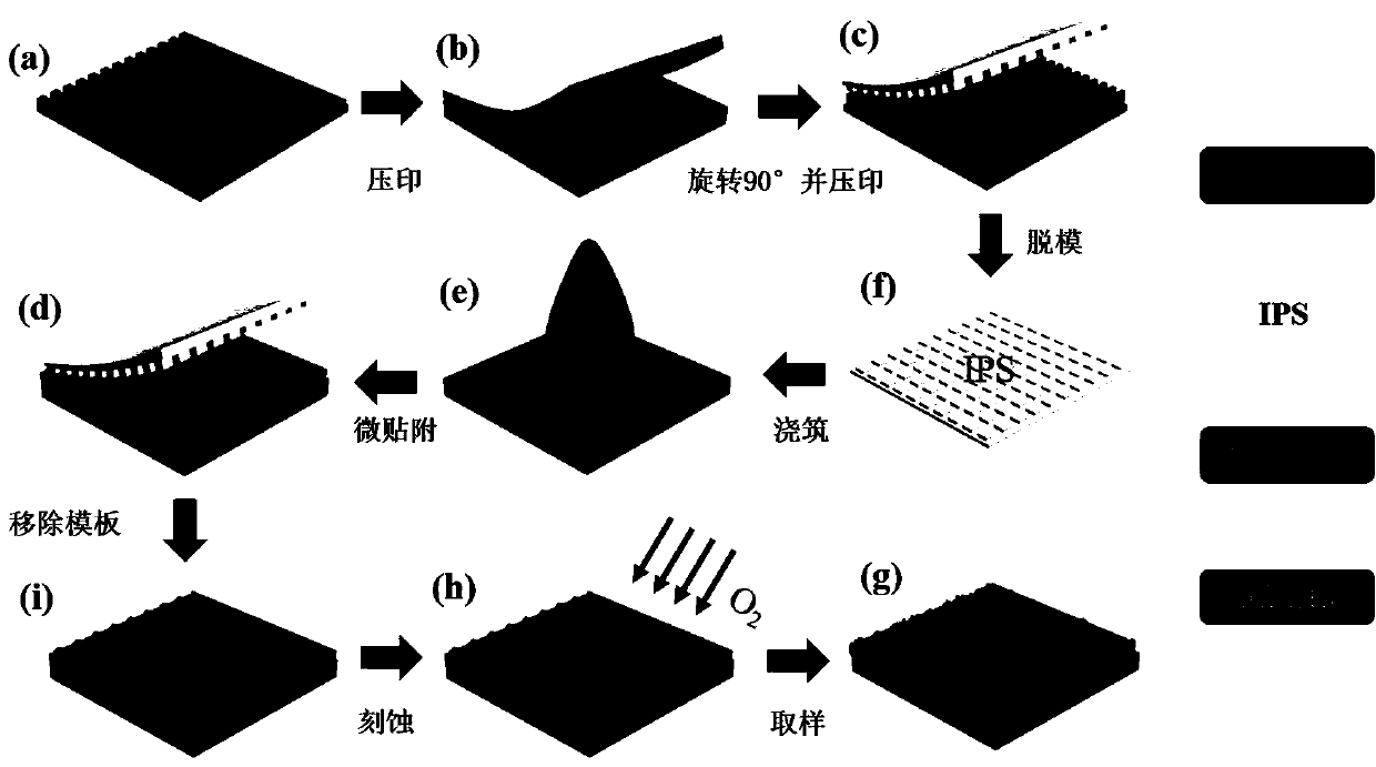
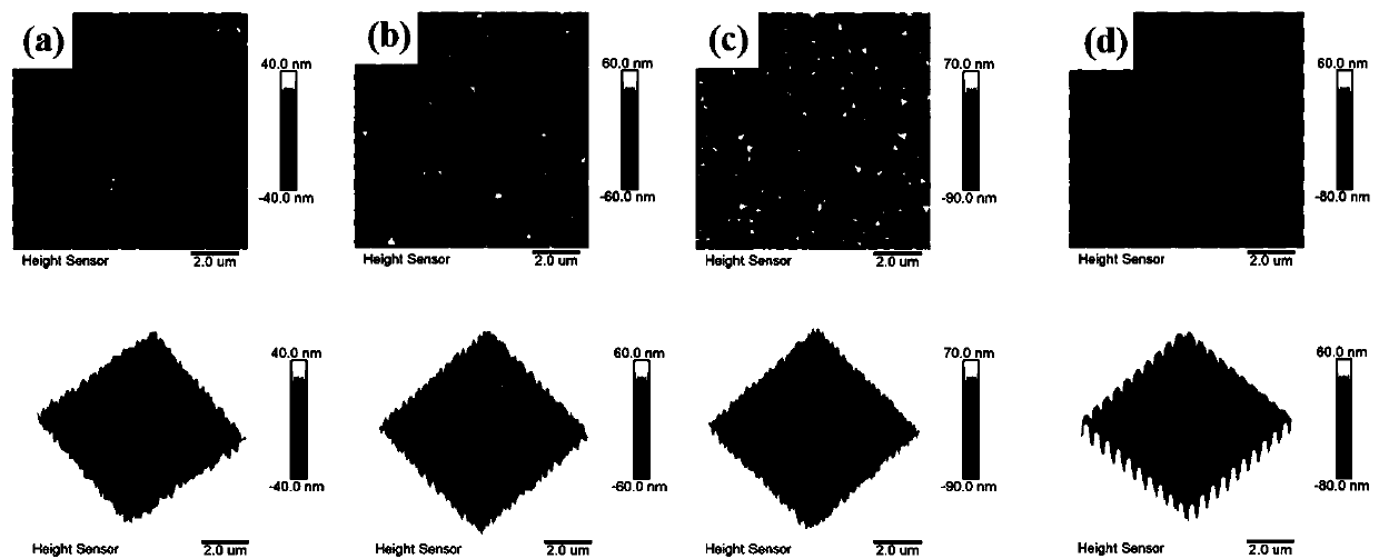
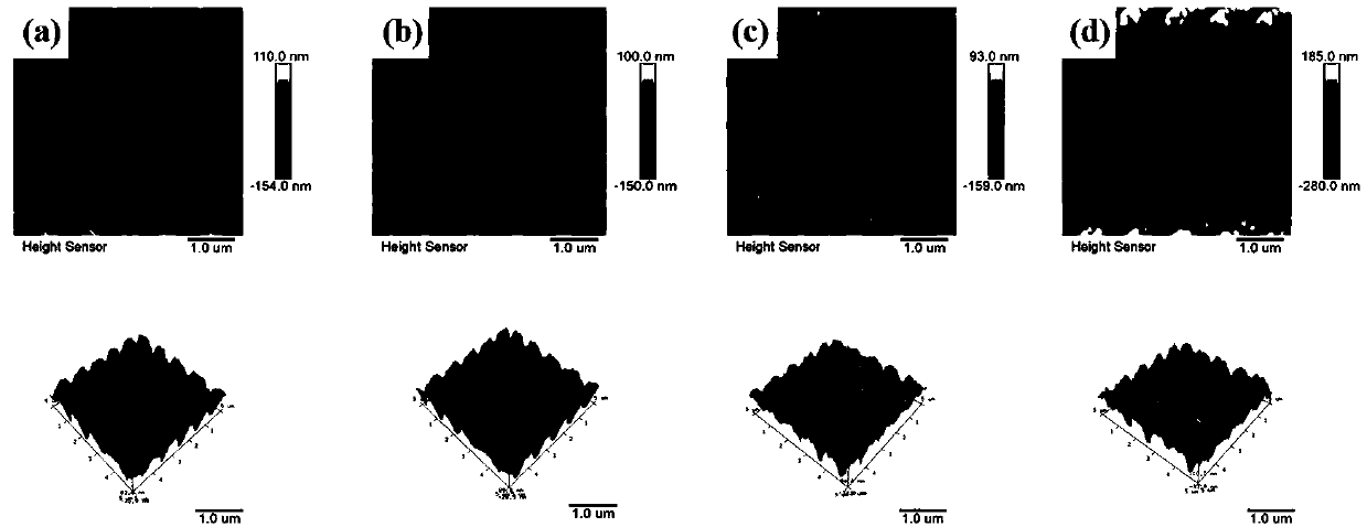
[0038] A method for preparing QLEDs enhanced by a composite structure, such as figure 1 shown, including the following steps:

[0039] (1) Spin-coat PEDOT:PSS layer, TFB layer, QDs layer and ZnO layer on the ITO side of the ITO glass substrate in turn, and then evaporate Al electrodes on the ZnO layer, and use curing glue to cure the Al electrodes to obtain the encapsulated QLED devices;

[0040] (2) The IPS template is a circle with a diameter of 8 cm. Cut it into four square structures with a size of 2.5 * 2.5 cm for use. Remove the protective layer on the IPS template and attach the side with the protective layer removed to the Si Then put the IPS template and the Si master into the center of the stage of the nanoimprinting instrument, and cover a layer of UV film on the IPS template as a protective layer, send the stage above the lifting platform and then lower it hatch, start the program for the first nanoimprinting, set the temperature of the first nanoimprinting at 15...

Embodiment 2

[0063] A method for preparing QLEDs enhanced by a composite structure, such as figure 1 shown, including the following steps:

[0064] (1) Spin-coat PEDOT:PSS layer, TFB layer, QDs layer and ZnO layer on the ITO side of the ITO glass substrate in turn, and then evaporate Al electrodes on the ZnO layer, and use curing glue to cure the Al electrodes to obtain the encapsulated QLED devices;

[0065] (2) The IPS template is a circle with a diameter of 8 cm. Cut it into four square structures with a size of 2.5 * 2.5 cm for use. Remove the protective layer on the IPS template and attach the side with the protective layer removed to the Si Then put the IPS template and the Si master into the center of the stage of the nanoimprinting instrument, and cover a layer of UV film on the IPS template as a protective layer, send the stage above the lifting platform and then lower it door, start the program for the first nanoimprinting, set the temperature of the first nanoimprinting at 145...

Embodiment 3

[0079] A method for preparing QLEDs enhanced by a composite structure, such as figure 1 shown, including the following steps:

[0080] (1) Spin-coat PEDOT:PSS layer, TFB layer, QDs layer and ZnO layer on the ITO side of the ITO glass substrate in turn, and then evaporate Al electrodes on the ZnO layer, and use curing glue to cure the Al electrodes to obtain the encapsulated QLED devices;

[0081] (2) The IPS template is a circle with a diameter of 8 cm. Cut it into four square structures with a size of 2.5 * 2.5 cm for use. Remove the protective layer on the IPS template and attach the side with the protective layer removed to the Si Then put the IPS template and the Si master into the center of the stage of the nanoimprinting instrument, and cover a layer of UV film on the IPS template as a protective layer, send the stage above the lifting platform and then lower it door, start the program for the first nanoimprinting, set the temperature of the first nanoimprinting at 155...


PUM

PropertyMeasurementUnit
depthaaaaaaaaaa
widthaaaaaaaaaa
heightaaaaaaaaaa

Abstract

The invention provides a QLED device with an enhanced composite structure and a preparation method of the QLED device. The light emitting efficiency of a positive QLED device is improved through a micro-nano structure composite structure constructed by a nano grid structure composite folded structure. The composite structure is constructed on the basis of the nanoimprint technology, the micro-attachment technology and the surface plasma etching technology, and the method comprises the steps: preparing a nanoimprint template and processing the transferred pattern again. An IPS polymer is used as a nano-imprinting template through the nano-imprinting technology, and the template pattern is transferred to the PDMS dielectric layer through the micro-attachment technology; on the basis, the composite structure is constructed on the glass substrate through the surface plasma etching technology to enhance light emitting of the QLED substrate. The QLED device with the enhanced composite structure can have the highest brightness and efficiency, and the brightness and the EQE are improved by 46% at most compared with conventional devices; and the construction mode of the composite structureis simple, the cost is low, and industrial popularization and application are facilitated.

Description

technical field [0001] The invention belongs to the field of QLED display and lighting, and in particular relates to a composite structure enhanced QLED device and a preparation method thereof. Background technique [0002] In the field of display and lighting, light-emitting diodes are one of the most important components. Although the existing OLEDs have been commercialized, they are limited by factors such as the easy decomposition of organic matter by heat and the stability and lifespan. QLED is attracting attention. A new generation of display and lighting products. At present, the external quantum efficiency of conventional QLED devices has been improved to approach the theoretical maximum value, but this value still cannot meet the needs of commercial applications. The problem of the reason is the problem of light extraction. Due to the waveguide mode, surface plasmon mode, and substrate mode caused by the internal total reflection of the QLED device, a large amount ...

Claims


Application Information

Patent Timeline
Patent Type & Authority Applications(China)
IPC IPC(8): H01L51/52H01L51/56
CPCH10K50/854H10K50/858H10K71/00
Inventor 杜祖亮王书杰李晨冉王啊强方岩
Owner HENAN UNIVERSITY
Why Eureka
Try Eureka