Method of manufacturing mechanical blind half hole

A production method and technology of blind holes, which are applied in the fields of printed circuit manufacturing, electrical connection formation of printed components, electrical components, etc., can solve the problems of complex production process, easy production error, and inability to etch the front, so as to optimize the process production process, The effect of avoiding capes and burrs and saving the tinning process

Active Publication Date: 2019-08-13
JIANGMEN SUNTAK CIRCUIT TECH
View PDF10 Cites 3 Cited by
  • Summary
  • Abstract
  • Description
  • Claims
  • Application Information

AI Technical Summary

Problems solved by technology

[0005] 1. The added one-time electroplating process needs to be produced on the graphic electroplating line, which makes the production process complicated, greatly increases the production cost, and is prone to production errors;
[0006] 2. In the SET shape, the bottom of the mechanical blind hole is easy to oxidize. When electro-tinning is performed, there is no micro-etching process, which will easily lead to poor tin plating at the bottom of the mechanical blind hole, and cannot effectively protect the copper layer at the bottom of the mechanical blind hole;
[0007] 3. When the shape of the gong set is shaped, a cape will be formed on the edge of the board. After tinning, the cape will be protected by the tin layer. When the outer layer is etched, the cape cannot be etched away, resulting in short circuit and scrapping

Method used


Image

  • Method of manufacturing mechanical blind half hole
  • Method of manufacturing mechanical blind half hole

Examples


Embodiment

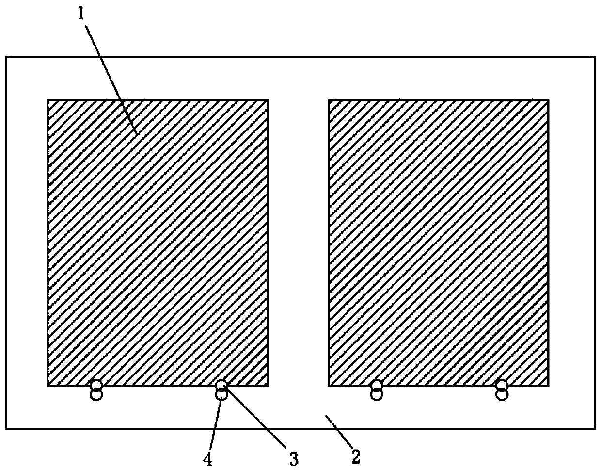
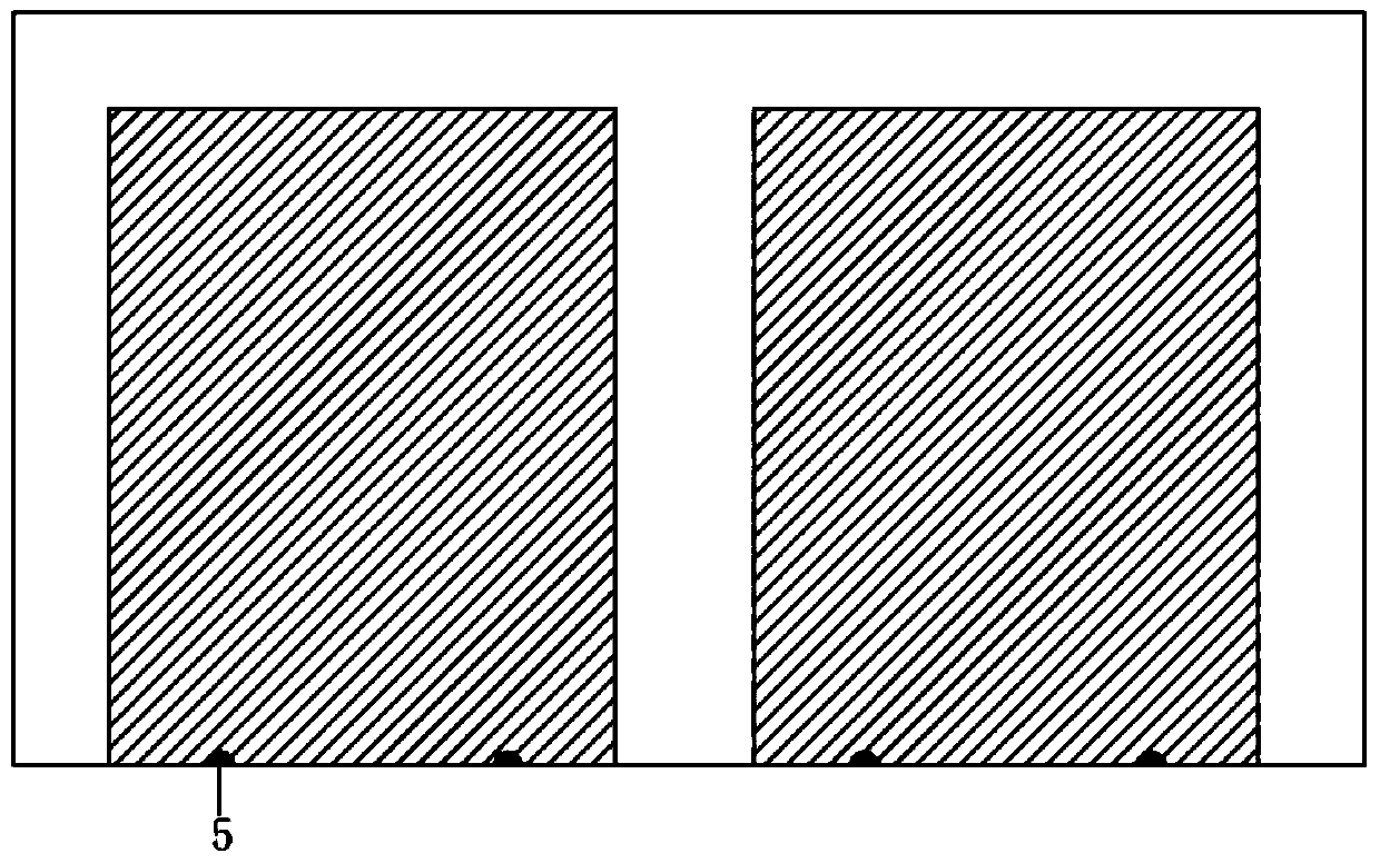
[0025] This embodiment provides a method for manufacturing a circuit board, which includes a method for manufacturing mechanical blind and half holes. The specific process is as follows:

[0026] (1) Cutting: cut out the core board according to the board size 520mm×620mm, the thickness of the core board is 0.8mm, and the thickness of the outer layer of copper foil is 1OZ.

[0027] (2) Inner layer circuit production (negative film process): Inner layer graphics transfer, use a vertical coating machine to coat a photosensitive film on the core board, the film thickness of the photosensitive film is controlled at 8 μm, and a fully automatic exposure machine is used to 5-6 grids The exposure ruler (21-grid exposure ruler) completes the exposure of the inner layer circuit on the core board, and after development, the inner layer circuit pattern is formed on the core board; the inner layer is etched, and the inner layer circuit is etched out of the exposed and developed core board, a...


PUM


Abstract

The invention discloses a method for manufacturing a mechanical blind half hole, and the method comprises the following steps: drilling a blind hole at the edge of a unit plate area on a production board, wherein a half of the blind hole is located in a forming line area on the production plate; drilling a through hole with the same aperture as the blind hole in the forming line area beside the blind hole, wherein the through hole is intersected with the blind hole; metalizing the hole through the processes of copper deposition and full-board electroplating; manufacturing an outer-layer circuit on the production board, firstly milling off the forming line area beside the blind hole in the production board in the process of manufacturing the outer-layer circuit after pattern electroplating,and then performing outer-layer etching to obtain the outer-layer circuit and the metalized blind half-hole. According to the invention, the risk that the bottoms of the blind hole semi-holes are free of copper can be effectively solved through the optimization of the production process, the problems of shawl and burrs on the edges of the blind hole semi-holes can be avoided, and the quality of circuit board products is guaranteed.

Description

technical field [0001] The invention relates to the technical field of manufacturing printed circuit boards, in particular to a method for manufacturing mechanical blind and half holes. Background technique [0002] Existing printed circuit board products meet the requirements of mounting components on the edge of the board, and the components only conduct part of the circuit layer on the printed circuit board, so it is necessary to design metallized blind holes and half holes (that is, semicircular holes) on the edge of the board. Blind holes) for mounting components. [0003] Due to the problem of the tinning ability of graphic electroplating, the copper at the bottom of the mechanical blind hole cannot be tinned smoothly to form an etching protection. As a result, when the outer layer is etched, the copper at the bottom of the mechanical blind hole is etched away, resulting in no copper at the bottom of the mechanical blind hole scrapped. Therefore, the conventional met...

Claims


Application Information

Patent Timeline
Patent Type & Authority Applications(China)
IPC IPC(8): H05K3/00H05K3/42
CPCH05K3/0047H05K3/421
Inventor 白亚旭曹雪春钟君武张雪松高赵军
Owner JIANGMEN SUNTAK CIRCUIT TECH
Why Eureka
Try Eureka