Low junction capacitance characteristic terahertz Schottky diode and manufacturing method thereof

A low junction capacitance and diode technology, applied in the field of low junction capacitance terahertz Schottky diodes and their fabrication, can solve problems such as low cutoff frequency of Schottky diodes, and achieve the effect of small device capacitance and high cutoff frequency

Inactive Publication Date: 2019-08-16
SUN YAT SEN UNIV
View PDF2 Cites 8 Cited by
  • Summary
  • Abstract
  • Description
  • Claims
  • Application Information

AI Technical Summary

Problems solved by technology

[0004] The purpose of the present invention is to provide a terahertz Schottky diode with low junction capacitance characteristics and its manufacturing method, so as to solve the problem of low cut-off frequency of the existing Schottky diode

Method used


Image

  • Low junction capacitance characteristic terahertz Schottky diode and manufacturing method thereof
  • Low junction capacitance characteristic terahertz Schottky diode and manufacturing method thereof
  • Low junction capacitance characteristic terahertz Schottky diode and manufacturing method thereof

Examples


Embodiment 1

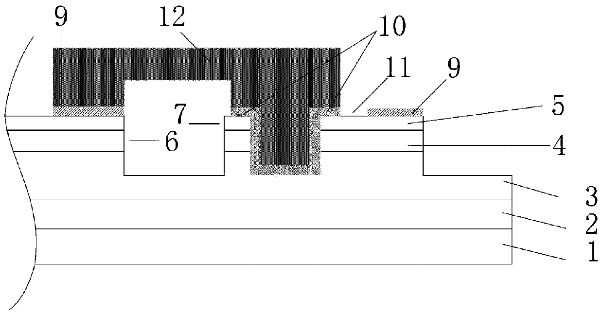
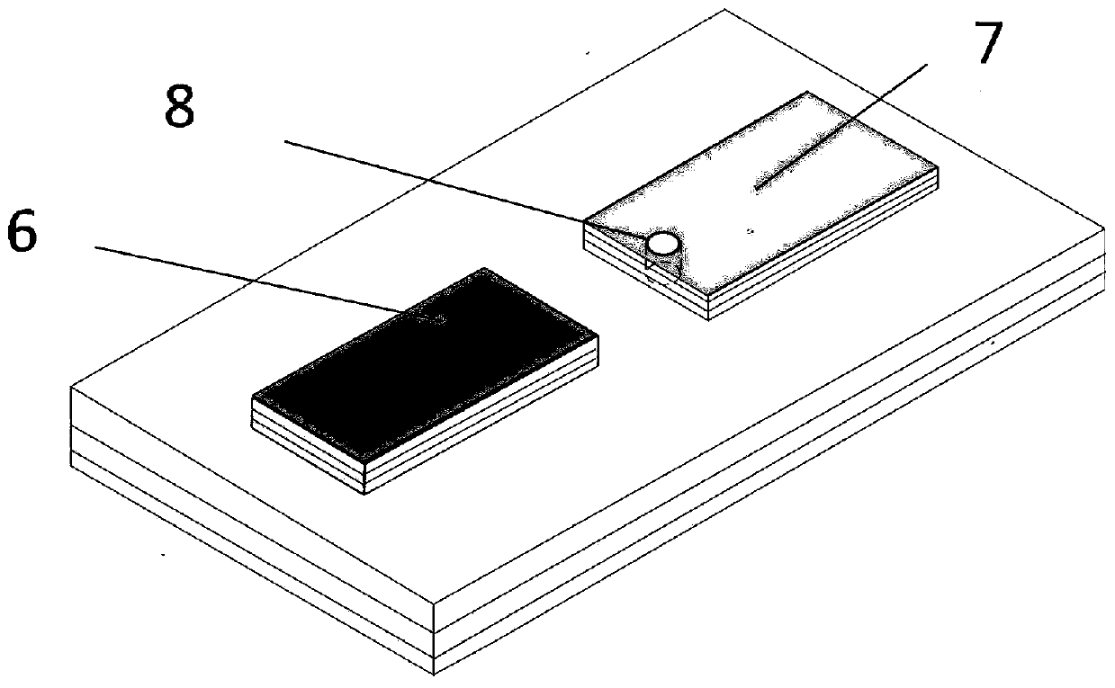
[0064] Such as Figure 1-Figure 6 As shown, a terahertz Schottky diode device with low junction capacitance characteristics, wherein, from bottom to top, there are substrate 1, stress buffer layer 2, gallium nitride GaN channel layer 3, aluminum gallium nitride AlGaN potential Barrier layer 4, gallium nitride GaN cap layer 5; there are two convex surfaces (first convex surface 7 and second convex surface 6) on the gallium nitride GaN channel layer 3, and the convex surface includes part of the gallium nitride GaN channel layer 3 and aluminum gallium nitride AlGaN barrier layer 4 and gallium nitride GaN capping layer 5; there is a cylindrical hole 8 on the surface of the first convex surface 7, and the depth is consistent with the height of the convex surface; two layers of different Schottky metals 10 and The ohmic contact metal 9, the Schottky metal 10 is separated from the ohmic contact metal 9 by a channel 11; the Schottky contact metal 10 leads out a hollow air bridge 12 i...

Embodiment 2

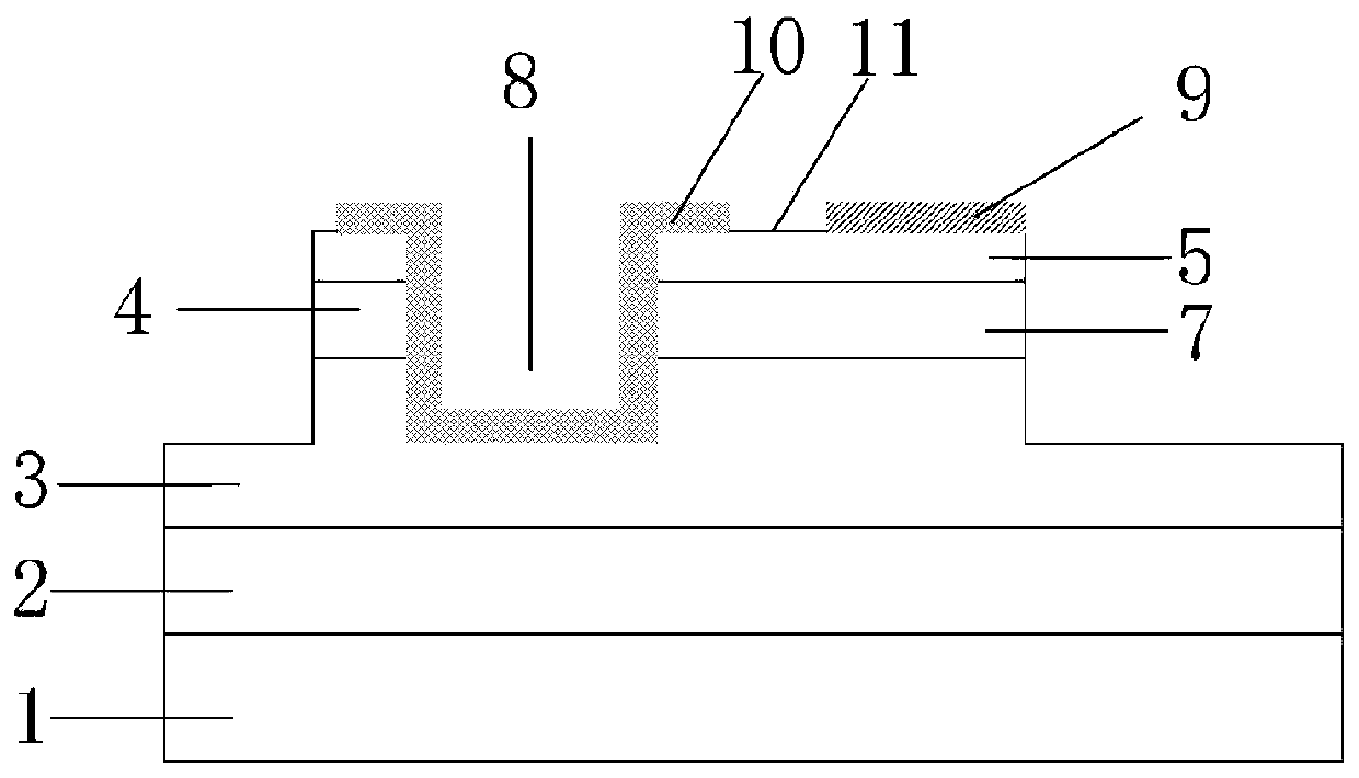
[0066] This embodiment is similar to embodiment 1, as Figure 7 As shown, the difference is that the Schottky metal 10 is made on the sidewall of AlGaN / GaN and on GaN. The process can be achieved, and it is also the performance to achieve low junction capacitance.

[0067] Compared with the prior art, the beneficial effect is: the present invention provides a terahertz Schottky diode with low junction capacitance characteristics and its manufacturing method, further, the Schottky contact metal 10 is nickel metal. There are two parts of capacitance in the contact between metal and material. Under zero bias, one is the capacitance that exists when the metal is in contact with the surface of the material, and this part of capacitance is relatively large; the other is when the metal is in contact with the two-dimensional electron gas. The Schottky junction formed between the materials has a depletion effect on the two-dimensional electron gas. There is a certain distance between ...


PUM


Abstract

The invention discloses a low junction capacitance characteristic terahertz Schottky diode and a manufacturing method thereof. A Schottky junction formed between Schottky contact metal and a materialhas a depletion effect on a two-dimensional electron gas, an etched semi-through hole is etched to a channel layer and etches off the two-dimensional electron gas of the channel layer, and the Schottky contact metal on a first convex surface and ohmic contact metal on a second convex surface are communicated by an air bridge, so that the direct area between the two-dimensional electron gas and theSchottky contact metal is very small, and capacitance is very small; and compared with a device with the Schottky contact metal completely covering the material surface, the device is smaller in capacitance, has no change in resistance, and can obtain higher cutoff frequency. A frequency mixer and a frequency doubler prepared through the low junction capacitance characteristic terahertz Schottkydiode can achieve a spectrum reception and detection function in the terahertz band, and is used for an excellent terahertz source and a terahertz receiver.

Description

technical field [0001] The invention relates to the technical field of the terahertz frequency band of semiconductor chips, in particular to a terahertz Schottky diode with low junction capacitance characteristics and a manufacturing method thereof. Background technique [0002] Terahertz Schottky has the characteristics of strong nonlinear effect, easy integration, and normal temperature operation. When the cut-off frequency of the Schottky diode reaches terahertz, it can achieve frequency multiplication or mixing of high-frequency signals, and can be used as a terahertz signal source and signal detector. Compared with thermionic bolometers, triode mixers and Gunn diodes, which are suitable for terahertz bands, which require harsh conditions to work normally, Schottky diodes show obvious advantages. Solid-state electronic devices working at room temperature High Electron Mobility Transistor (HEMT) diodes made of gallium aluminum nitride AlGaN / gallium nitride GaN heterojunc...

Claims


Application Information

Patent Timeline
Patent Type & Authority Applications(China)
IPC IPC(8): H01L29/06H01L29/66H01L29/872
CPCH01L29/0603H01L29/66143H01L29/872
Inventor 张佰君杨隆坤王玲龙
Owner SUN YAT SEN UNIV
Why Eureka
Try Eureka