Three-dimensional flash memory based on vertical channels of two-dimensional semiconductor materials and preparation thereof

A two-dimensional semiconductor and flash memory technology, which is applied in semiconductor/solid-state device manufacturing, semiconductor devices, nanotechnology for materials and surface science, etc., can solve problems affecting device uniformity, low carrier mobility, and process Slow and other problems, to achieve the effect of reducing the operating read and write voltage, high carrier mobility, and accelerating the process

Inactive Publication Date: 2019-08-20
HUAZHONG UNIV OF SCI & TECH
View PDF4 Cites 11 Cited by
  • Summary
  • Abstract
  • Description
  • Claims
  • Application Information

AI Technical Summary

Problems solved by technology

In the structure of the three-dimensional flash memory, it is necessary to deposit the channel material after the deep hole etching is completed, so the epitaxial growth of single crystal silicon cannot be carried out.
In the previous process, the deposition of amorphous silicon is usually used to form the channel, and the deposition time of amorphous silicon is very long, and its carrier mobility is very low compared with single crystal silicon, so the on-state current that can be provided is very limited
In addition, the deep hole filling of amorphous silicon is usually filled by atomic deposition technology, and the process is slow, which will occupy most of the process time
With the increase in the number of three-dimensional flash memory stack layers, it is difficult to ensure the uniformity of deep hole filling, which seriously affects the uniformity of the device

Method used


Image

  • Three-dimensional flash memory based on vertical channels of two-dimensional semiconductor materials and preparation thereof
  • Three-dimensional flash memory based on vertical channels of two-dimensional semiconductor materials and preparation thereof
  • Three-dimensional flash memory based on vertical channels of two-dimensional semiconductor materials and preparation thereof

Examples


Embodiment Construction

[0034] In order to make the object, technical solution and advantages of the present invention clearer, the present invention will be further described in detail below in conjunction with the accompanying drawings and embodiments. It should be understood that the specific embodiments described here are only used to explain the present invention, not to limit the present invention. In addition, the technical features involved in the various embodiments of the present invention described below can be combined with each other as long as they do not constitute a conflict with each other.

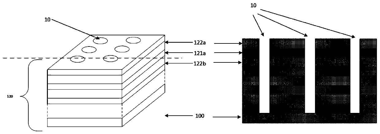
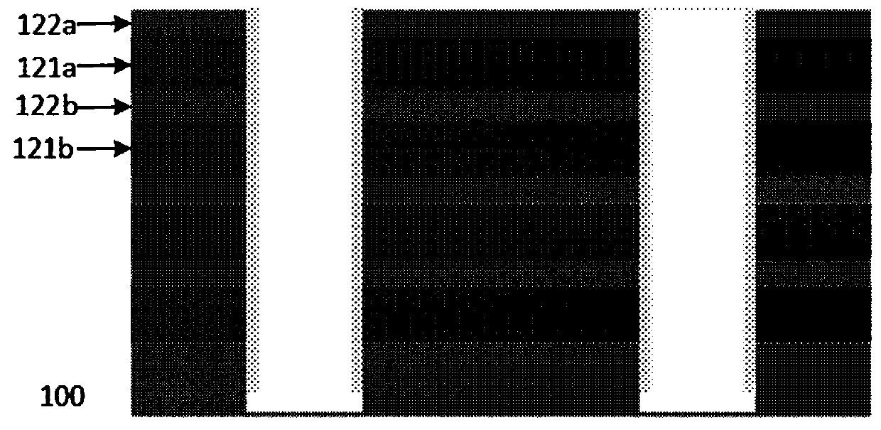
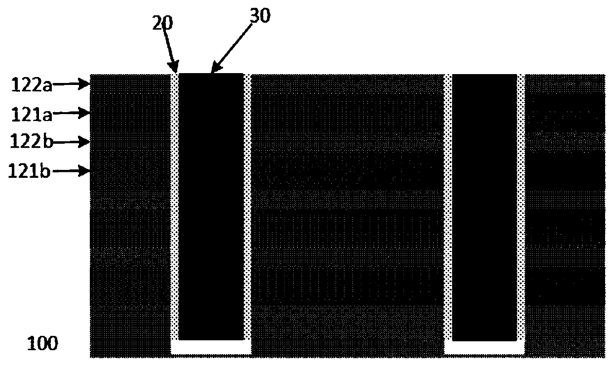
[0035] The present invention provides a three-dimensional semiconductor memory based on a vertical channel of a two-dimensional semiconductor material. The three-dimensional semiconductor memory includes a plurality of three-dimensional memory strings in the vertical direction, each three-dimensional memory string includes a semiconductor vertical channel, and the semiconductor vertical groove T...


PUM


Abstract

The invention belongs to the field of semiconductor memory manufacturing and particularly relates to a three-dimensional semiconductor memory based on vertical channels of two-dimensional semiconductor materials and a preparation method thereof. The three-dimensional semiconductor memory comprises a plurality of three-dimensional storage strings in a vertical direction, and each three-dimensionalmemory string includes a semiconductor vertical channel whose length is determined by the number of layers of memory three-dimensional stack. The vertical channel materials comprise one or more two-dimensional semiconductor materials and protection layers on the surfaces of the two-dimensional semiconductor materials. The protection layers are used for supporting and protecting the two-dimensionalsemiconductor materials, and the carrier mobility of the two-dimensional semiconductor materials is higher than that of amorphous silicon. According to the invention, the two-dimensional materials are used as memory channels, higher memory cell on-state current can be provided, and therefore, the operational power consumption of the memory is reduced.

Description

technical field [0001] The invention belongs to the field of semiconductor memory manufacturing, and more specifically relates to a three-dimensional semiconductor memory based on a vertical channel of a two-dimensional semiconductor material and its preparation. Background technique [0002] According to Moore's Law, the feature size of microelectronic devices continues to decrease, and there is a physical limit to the miniaturization of the special size of flash memory. Therefore, the planar flash memory technology begins to develop into three dimensions, and three-dimensional flash memory emerges as the times require. Compared with the traditional planar semiconductor memory, the storage density of the three-dimensional flash memory is no longer limited by the feature size of the process, and the storage density can be continuously improved by stacking in the vertical direction. The three-dimensional semiconductor memory used in the three-dimensional flash memory is compl...

Claims


Application Information

Patent Timeline
Patent Type & Authority Applications(China)
IPC IPC(8): H01L27/11568H01L27/11582H01L29/06H01L29/10H01L29/16H01L29/24H01L29/792H01L21/34B82Y30/00B82Y40/00
CPCH01L29/1606H01L29/24H01L29/1033H01L29/0665H01L29/66969H01L29/7926B82Y30/00B82Y40/00H10B43/30H10B43/27
Inventor 缪向水钱航童浩
Owner HUAZHONG UNIV OF SCI & TECH
Why Eureka
Try Eureka