Photoetching method for improving adhesion degree of photoresist and substrate

An adhesion and photoresist technology, applied in the field of photolithography, can solve the problems of increasing the occupation of the hot plate, uneven primer coating, large amount of hexamethyldisilazane, etc., to improve the adhesion, meet the The effect of process requirements

Pending Publication Date: 2019-08-23
ZHEJIANG CRYSTAL OPTECH
View PDF4 Cites 2 Cited by
  • Summary
  • Abstract
  • Description
  • Claims
  • Application Information

AI Technical Summary

Problems solved by technology

Generally, hot-plate priming with gas-phase bottoming film is used to improve the substrate surface, but this requires the modification of the glue coating machine to add modules and increase the occupation of the hot plate
Howeve...

Method used


Image

  • Photoetching method for improving adhesion degree of photoresist and substrate
  • Photoetching method for improving adhesion degree of photoresist and substrate

Examples


Embodiment 1

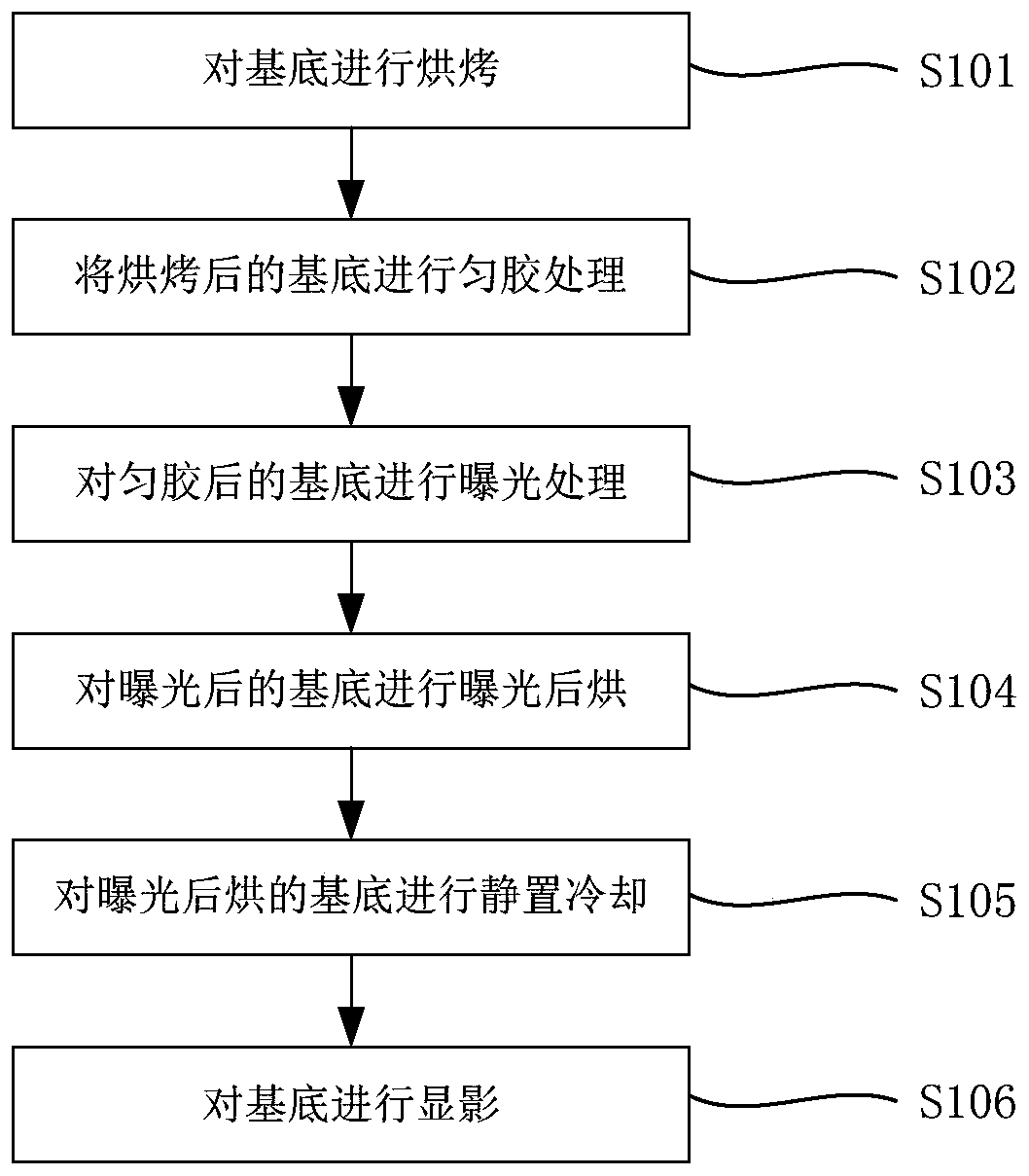
[0065] Such as figure 1 Shown, a kind of photolithography method that improves photoresist and substrate adhesion degree provided according to the present invention comprises:

[0066] Step S101, baking the substrate;

[0067] Step S102, performing glue leveling treatment on the baked substrate;

[0068] Step S103, performing exposure treatment on the substrate after uniform glue;

[0069] Step S104, performing post-exposure baking on the exposed substrate;

[0070] Step S105, standing and cooling the post-exposure baked substrate;

[0071] Step S106, developing the substrate.

[0072] The specific operation process is as follows:

[0073] First perform step S101 to bake the substrate, set the baking temperature to 160-180°C, and bake the time to 50-80s to increase the adhesion between the photoresist and the substrate; then proceed to step S102 to bake the substrate after baking Coating treatment; followed by step S103 to perform exposure treatment on the substratum aft...

Embodiment 2

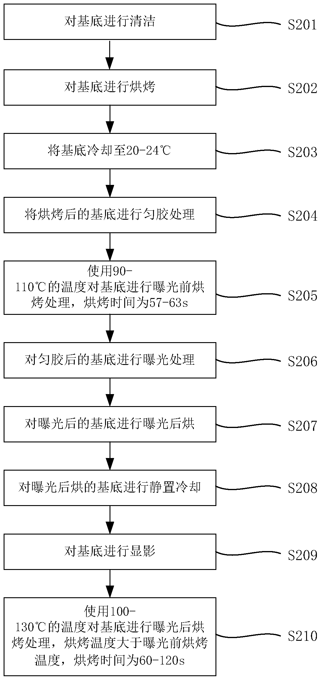
[0075] Such as figure 2 Shown, a kind of photolithography method that improves photoresist and substrate adhesion degree provided according to the present invention comprises:

[0076] Step S201, cleaning the substrate;

[0077] Step S202, baking the substrate;

[0078] Step S203, cooling the substrate to 20-24°C;

[0079] Step S204, performing glue leveling treatment on the baked substrate;

[0080] Step S205, using a temperature of 90-110°C to perform pre-exposure baking treatment on the substrate, and the baking time is 57-63s;

[0081] Step S206, performing exposure treatment on the substrate after uniform glue;

[0082] Step S207, performing post-exposure baking on the exposed substrate;

[0083] Step S208, standing and cooling the post-exposure baked substrate;

[0084] Step S209, developing the substrate;

[0085] In step S210, post-exposure baking is performed on the substrate at a temperature of 100-130° C., the baking temperature is higher than the pre-exposu...


PUM


Abstract

The invention provides a photoetching method for improving the adhesion degree of a photoresist and a substrate, and relates to the technical field of photoetching processes. The photoetching method for improving the adhesion degree of the photoresist and the substrate comprises the following steps: baking the substrate; carrying out glue homogenizing treatment on the baked substrate; carrying outexposure treatment on the substrate subjected to glue uniformization; carrying out exposure and drying on the exposed substrate; standing and cooling the substrate which is dried after exposure; anddeveloping the substrate. According to the photoetching method provided by the invention, a substrate surface tackifier does not need to be used, and the adhesion degree between the substrate and thephotoresist can be effectively improved by the baking of the substrate before homogenizing of the photoresist, the baking after exposure and the standing and cooling after baking, so that the processrequirement is met, and an equipment module does not need to be additionally added.

Description

technical field [0001] The invention relates to the technical field of photolithography technology, in particular to a photolithography method for improving the adhesion between photoresist and substrate. Background technique [0002] In the field of semiconductor technology and micro-nano processing, photolithography is an indispensable processing link. The traditional photolithography process includes three main processing steps: coating, exposure, and development. First, the photoresist is evenly coated on the surface of the substrate, then the mask pattern is exposed by an exposure machine, and finally the mask pattern is transferred from the mask plate to the substrate through development. [0003] In the photolithography process, substrate adhesion enhancement treatment is usually performed before the leveling process to increase the adhesion between the photoresist and the substrate, so as to avoid pattern deformation or peeling during the photolithography process. ...

Claims


Application Information

Patent Timeline
IPC IPC(8): G03F7/16G03F7/40
CPCG03F7/168G03F7/40
Inventor 陈瑶王波
Owner ZHEJIANG CRYSTAL OPTECH
Why Eureka
Try Eureka