Plasma sterilizing and disinfecting device and air purifier
A sterilization and disinfection device, plasma technology, applied in the direction of disinfection, deodorization, etc., can solve the problems of inability to achieve sterilization and disinfection, easy breakage of corona wire, high excitation voltage, etc., to solve the problem of bacterial growth, wide application range and long service life long effect
- Summary
- Abstract
- Description
- Claims
- Application Information
AI Technical Summary
Problems solved by technology
Method used
Image
Examples
Embodiment 1
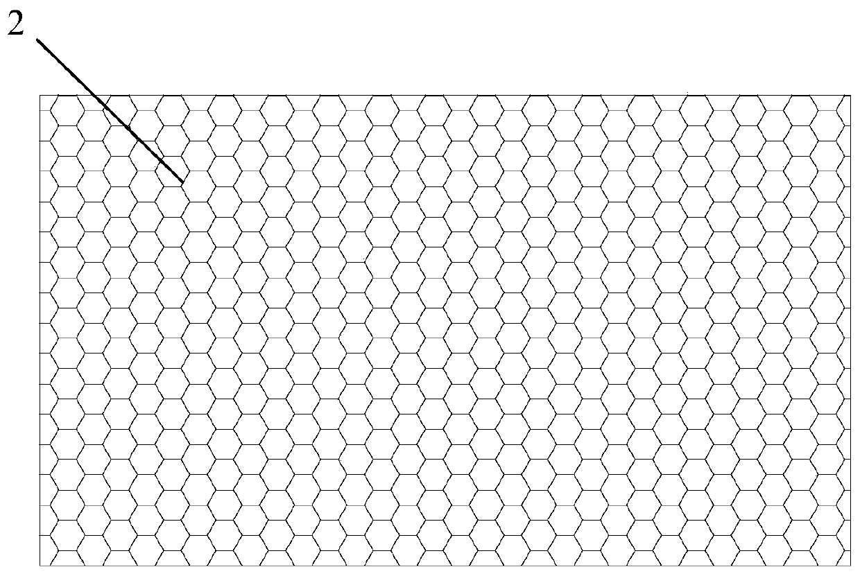
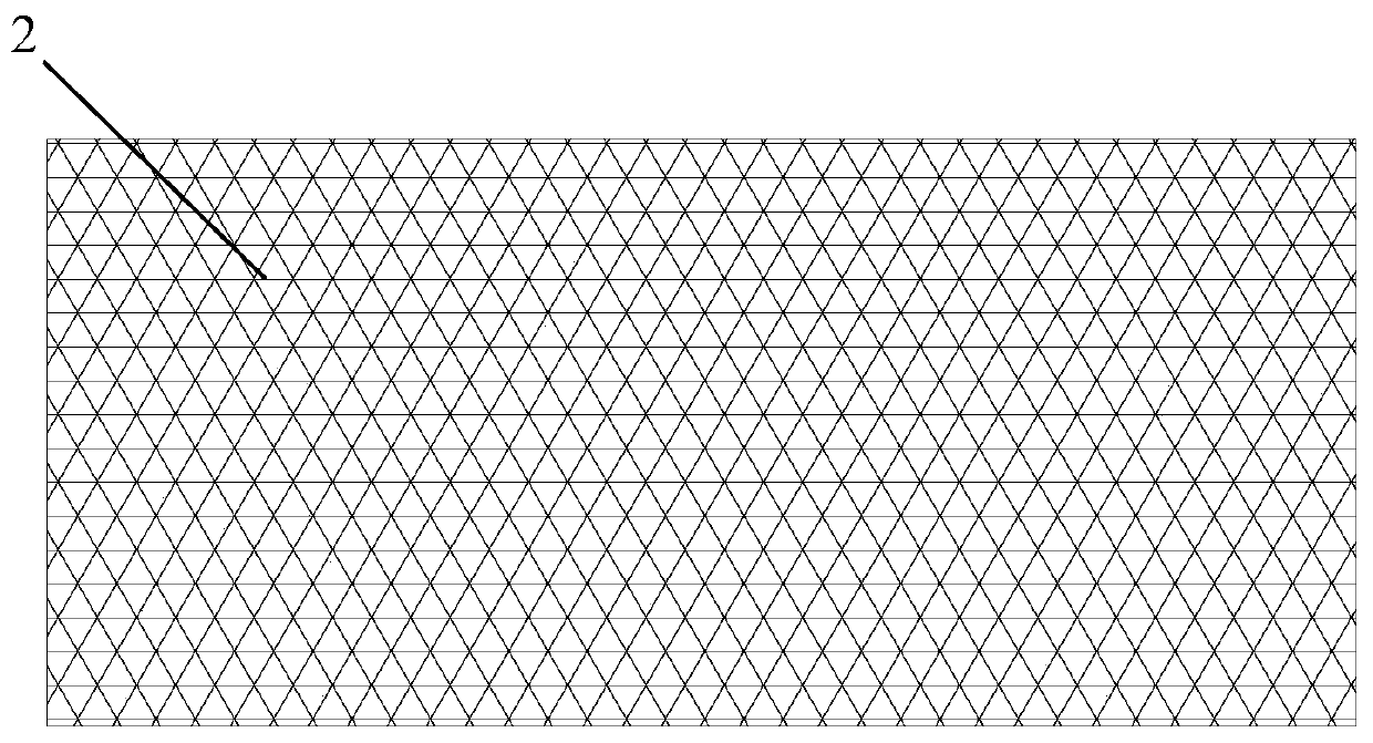
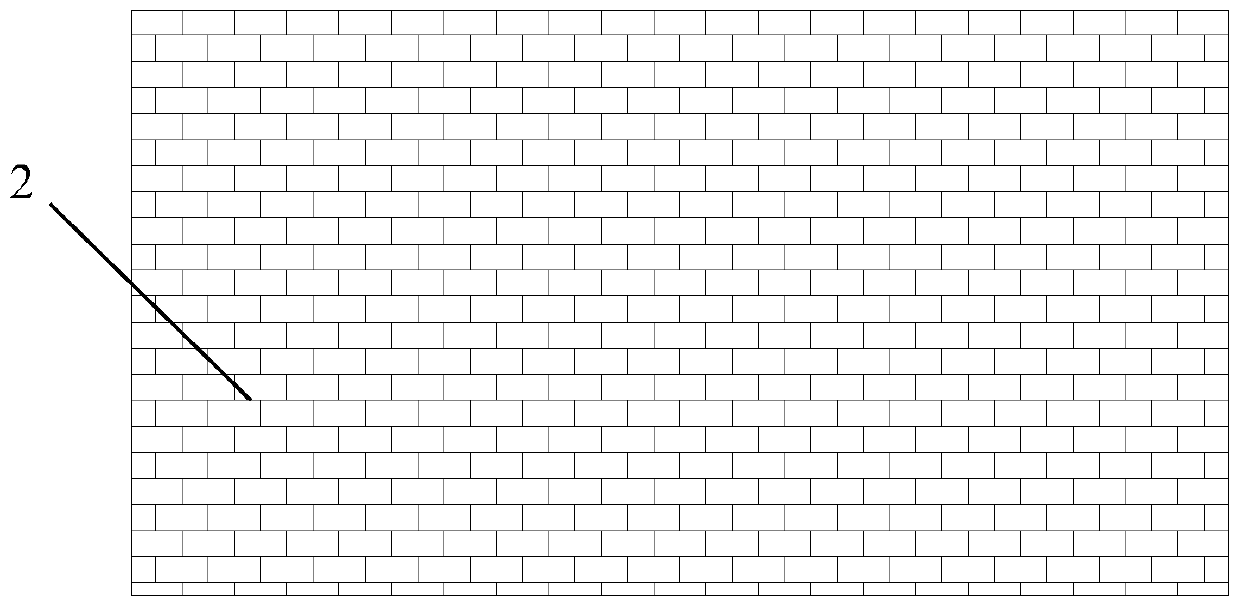
[0034] In the first embodiment, the conductive nano wire is composed of nanofiber bundles 2, which are formed by mixing and winding two or more kinds of soft nanowires, and have good electrical conductivity. The nanofiber bundle 2 forms a porous, mesh-like flexible fiber web by weaving, such as figure 1 , figure 2 with image 3 As shown, the flexible fiber net can be woven into a network structure of hexagonal holes, or can be woven into a network structure of triangular holes or rectangular holes. In this embodiment, the hole shape of the network structure is not particularly limited. Of course, the nano conductive filament can also be composed of only one kind of conductive nano wire.
[0035] Further, the nanowires can be nanoscale carbon fibers, nanoscale metal wires or other nanoscale materials.
[0036] Since the nanofiber bundles 2 have good electrical conductivity, and the flexible fiber web is woven from thousands of nanofiber bundles 2, the flexible fiber web can...
Embodiment 2
[0038] In the second embodiment, the ionization component 1 uses the flexible circuit board as the base material, and etches the nano-scale conductive material (such as nano-scale metal material) onto the surface of the flexible circuit board through the etching process to form a nano-scale A network or other shape structure, that is, a nano-conductive grid. Such as Figure 4 As shown, the nano conductive grid formed by etching can specifically be a dendritic bifurcated structure 3, of course, it can also be figure 1 , figure 2 with image 3 The triangular, rectangular and hexagonal grid structures shown in , the shape of the nano conductive grid formed by etching is not particularly limited in this embodiment.
[0039] In addition, the base material of the ionization component 1 may also adopt a plate structure made of porous material.
[0040] In addition, the processing technology for forming nano-conductive grids on the surface of the substrate is not limited to etchi...
PUM
 Abstract
Description
Claims
Application Information
 - R&D
- Intellectual Property
- Life Sciences
- Materials
- Tech Scout
- Unparalleled Data Quality
- Higher Quality Content
- 60% Fewer Hallucinations
Browse by: Latest US Patents, China's latest patents, Technical Efficacy Thesaurus, Application Domain, Technology Topic, Popular Technical Reports.
© 2025 PatSnap. All rights reserved.Legal|Privacy policy|Modern Slavery Act Transparency Statement|Sitemap|About US| Contact US: help@patsnap.com


