Method for realizing ultra-wideband light absorption and a composite micro-structure

A composite microstructure, ultra-broadband technology, applied in optics, optical components, instruments, etc., can solve the problems of limited number of microstructure resonance units and increase the difficulty of preparation, and achieve high polarization-insensitive broadband absorption performance, excellent broadband light Absorption performance, the effect of enhancing absorption efficiency

Active Publication Date: 2019-09-03
JIANGNAN UNIV
View PDF26 Cites 17 Cited by
  • Summary
  • Abstract
  • Description
  • Claims
  • Application Information

AI Technical Summary

Problems solved by technology

However, for multi-band metamaterial broadband absorbers, it is necessary to integrate two or more microstructure resonant units in one structural unit, which not only increases the difficulty of preparation, but also increases the number of microstructure resonant units that can actually be accommodated in one structural unit. The number is limited; for the hyperbolic metamaterial structure, in order to effectively use the slow optical waveguide mode to expand the bandwidth of light absorption, the structural unit often needs a gradually changing microstructure width, that is, the width of the microstructure in a structural unit increases with its own depth. increase, which brings great challenges to the fabrication of devices

Method used


Image

  • Method for realizing ultra-wideband light absorption and a composite micro-structure
  • Method for realizing ultra-wideband light absorption and a composite micro-structure
  • Method for realizing ultra-wideband light absorption and a composite micro-structure

Examples


Embodiment 1

[0038] Example 1: Designing an ultra-broadband absorber in the visible light-near-infrared band using metal / dielectric composite microstructure

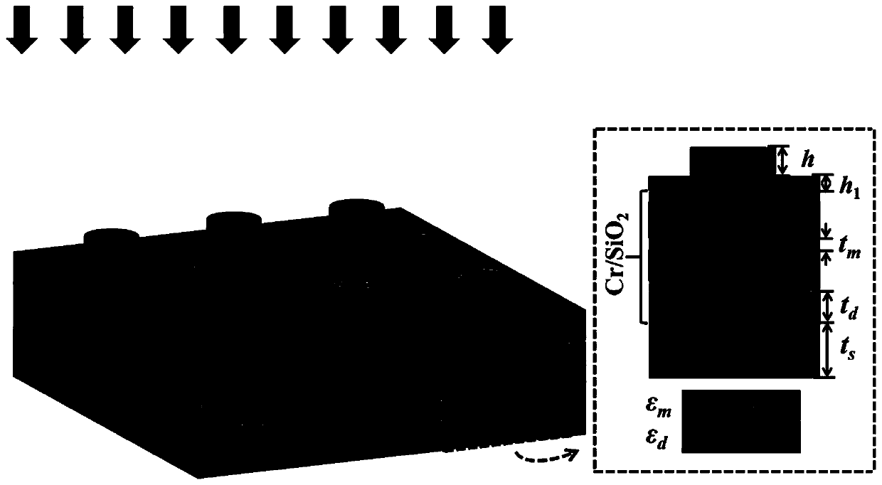
[0039] Visible-near-infrared band ultra-broadband absorber is designed by metal / dielectric composite microstructure, the schematic diagram is as follows figure 1 shown. figure 1 It is a schematic diagram of metal / dielectric composite microstructure in an embodiment of the present invention, the selected metal microstructure is a nano-column array, and the selected metal and dielectric materials are respectively chromium (Cr) and silicon dioxide (SiO 2 ). where P is the period of the nanopillar array, d is the diameter of the nanopillar, h is the height of the nanopillar, h 1 for SiO 2 The thickness of the buffer layer, there are 3 pairs of Cr / SiO 2 Multilayer film stack, t m is the thickness of metal Cr film, t d for SiO 2 The thickness of the dielectric film layer, the substrate is a Cr thin film with a sufficiently large opt...

Embodiment 2

[0042] Example 2: Broadband near-field reflection and light field localization caused by metal-dielectric periodic film stacks

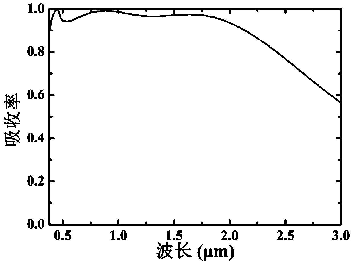
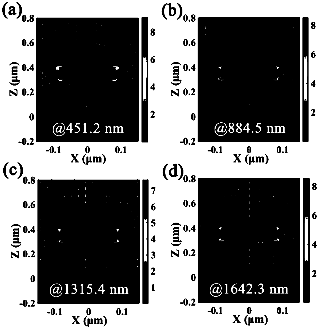
[0043] Based on the calculation results of Example 1, in order to clarify the broadband light absorption mechanism corresponding to this structure, in figure 2 Under the parameter condition of , in the wavelength band of broadband light absorption, four light absorption wavelengths with large differences are selected in sequence along the wavelength increasing direction, and the normalized electric field intensity distribution and energy flow direction corresponding to the structure are calculated by the strict coupled wave method distribute, get image 3 .

[0044] image 3 It is the normalized electric field intensity distribution and energy flow direction distribution of different wavelengths in an embodiment of the present invention, wherein the chromaticity bar represents the amplitude of the normalized electric field intensity, the arrow ind...

Embodiment 3

[0046] Example 3: Angle-insensitive absorption phenomenon of metal / dielectric composite microstructure ultra-broadband absorber

[0047] Based on the metal / dielectric composite microstructure ultra-broadband absorber in Example 1, when the structural parameters are unchanged, the incident angle is changed, and the strict coupled wave method is used to calculate the variation of the absorption spectrum with the incident angle for TM polarization and TE polarization respectively. curve, get Figure 4 .

[0048] Figure 4 In one embodiment of the present invention, the absorption spectrum varies with the incident angle, and the structural parameters and figure 2 same. (a) corresponds to TM polarization; (b) corresponds to TE polarization. From Figure 4 It can be seen that when the incident angle increases from 0° to 60°, the absorber still has broadband light absorption effect. Especially, for the TM polarization case, when the incident angle increases to 60°, the light a...


PUM

PropertyMeasurementUnit
thicknessaaaaaaaaaa

Abstract

The present invention discloses a method for realizing ultra-wideband light absorption and a composite micro-structure. The method combines a metal-medium periodic film stack with a metal micro-structure array, namely, carries a metal micro-structure array above a conventional metal-medium periodic film stack, combines wide-band near-field reflection provided by the metal-medium periodic film stack and surface plasmon resonance effect of the metal micro-structure array, to achieve ultra-wideband light absorption enhancement in a visible-near infrared band. In addition, a broadband absorbing device designed by the method does not require use of precious metals such as gold or silver, has relatively low preparation costs, has superior polarization-insensitive broadband absorption performanceand extremely high manufacturing tolerances, and has great application prospects in the fields of enhanced nano imaging, stealth materials, solar cells, light modulators, and touch screens.

Description

technical field [0001] The invention relates to the fields of micro-electromechanical systems, photovoltaic solar energy, and photoelectric detection, in particular to a method for realizing ultra-broadband light absorption and a metal / medium composite microstructure. Background technique [0002] Metamaterial wave absorbers can use different resonance modes or light field coupling effects in micro-nano structures, such as: surface plasmon resonance, guided mode resonance, Fano resonance, electromagnetically induced transparency, etc., to enhance the light absorption efficiency of metamaterial devices . This type of absorbing device is often based on a metal / dielectric composite structure. By adjusting structural parameters, such as adjusting the surface shape, size, arrangement, and orientation of structural units, etc., localized light field and electromagnetic field enhancement effects are generated in the microstructure to achieve light absorption. Enhanced efficiency. ...

Claims


Application Information

Patent Timeline
Patent Type & Authority Applications(China)
IPC IPC(8): G02B5/00
CPCG02B5/003G02B5/008
Inventor 桑田齐红龙尹欣王勋李国庆王跃科
Owner JIANGNAN UNIV
Why Eureka
Try Eureka