Method for realizing ultra-wideband light absorption enhancement by adopting composite microstructure

A composite microstructure and light absorption technology, applied in optics, optical components, instruments, etc., can solve the problems of increasing difficulty, large microstructure depth, and many film pairs, and achieve excellent broadband light absorption performance and high absorption efficiency. Effect

Active Publication Date: 2020-06-26
JIANGNAN UNIV
View PDF10 Cites 8 Cited by
  • Summary
  • Abstract
  • Description
  • Claims
  • Application Information

AI Technical Summary

Problems solved by technology

However, although this type of microstructure can further expand the light absorption bandwidth, due to the large number of film pairs required, the depth of the microstructure is large, especially its gradual microstructure width, which significantly increases the difficulty of practical preparation.

Method used


Image

  • Method for realizing ultra-wideband light absorption enhancement by adopting composite microstructure
  • Method for realizing ultra-wideband light absorption enhancement by adopting composite microstructure
  • Method for realizing ultra-wideband light absorption enhancement by adopting composite microstructure

Examples


Embodiment 1

[0024] Example 1: Visible light to near-infrared band ultra-broadband absorber designed with composite microstructure

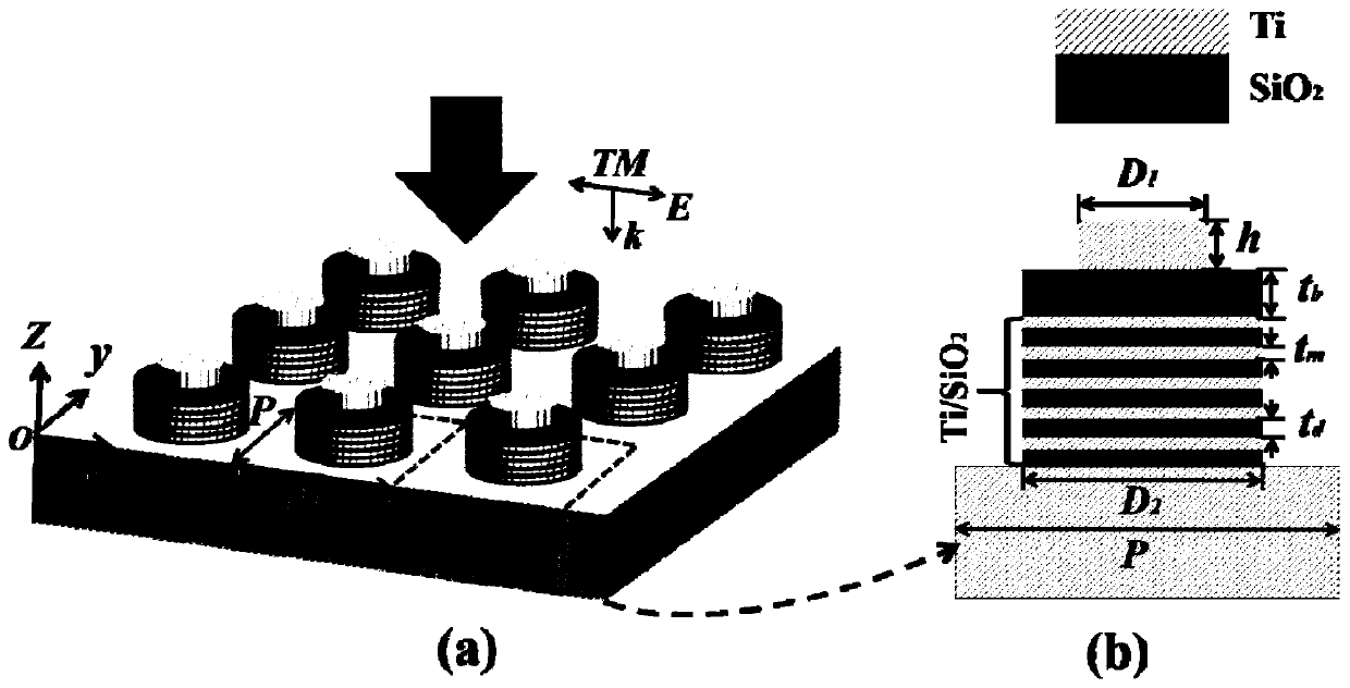
[0025] 11. The composite microstructure is used to design the ultra-broadband absorber in the visible light to near-infrared band. The schematic diagram of its structure is shown in figure 1 shown. The selected metal and dielectric materials are titanium (Ti) and silicon dioxide (SiO 2 ), since the structure is a periodic structure, for a cell, it consists of a Ti cylinder and Ti / SiO 2 Multilayer film cylinders are cascaded, and the diameter of the Ti cylinders is smaller than that of Ti / SiO 2 The diameter of the multilayered cylinder with SiO between the Ti cylinder and the multilayered cylinder 2 Medium buffer layer. The height and diameter of the Ti cylinder are h and D respectively 1 , the thickness and diameter of the buffer layer are t b and D 2 , Ti and SiO in a multilayer film cylinder 2 The thickness is t m and t d , the diameter of the mul...

Embodiment 2

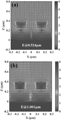
[0028] Example 2: Electric field localization and energy flow distribution of composite microstructures

[0029] Based on the calculation results of Example 1, in order to better understand the ultra-broadband strong light absorption mechanism of the structure, the electric field and energy flow distribution at the three resonant absorption peaks were studied. Other parameters of the structure are the same as in Example 1, and the corresponding wavelengths are respectively 524nm, 1001nm, 1952nm, such as image 3 shown.

[0030] from image 3 It can be seen that at short wavelengths (524nm), the electric field is mainly localized around the Ti cylinder and produces significant enhancement, showing a surface plasmon resonance mode, and the incident light field circulates along the surface of the Ti cylinder, thereby causing surface plasmons Enhanced bulk resonance absorption. At the long wavelength (1952nm), the electric field is mainly localized in the cavity between the mul...

Embodiment 3

[0031] Example 3: Effect of Ti cylinder size change on broadband absorption characteristics

[0032] Based on the composite microstructure ultra-broadband absorber of Example 1, under the parameter conditions of Example 1, for the case of normal incidence, the Ti cylinder height h and the Ti cylinder height diameter D are calculated using the finite time domain difference method 1 The absorption spectrum of the absorber when the change occurs, we get Figure 4 .

[0033] Such as Figure 4 As shown in (a), when there is no Ti cylinder (h = 0), the broadband high absorption performance of the structure is poor. The introduction of Ti cylinders can improve the light absorption efficiency in a wide range of wavelengths, but with the increase of the height of Ti cylinders, the absorption performance tends to be saturated. When the height of the Ti column exceeds 140 nm, the light absorption rate decreases. Therefore, when the height of Ti cylinders is 140 nm, the structure has ...


PUM


Abstract

The invention discloses a method for realizing ultra-wideband light absorption enhancement by adopting a composite microstructure, and belongs to the field of solar cells, thermal emitters and photoelectric detection. A cell of the composite microstructure is formed by cascading a Ti cylinder with a small diameter and a Ti / SiO2 multilayer film cylinder, and is provided with a metal substrate. Short-wavelength light waves are absorbed through resonance of surface plasmas excited around the Ti cylinder; long-wavelength light waves are absorbed through plasma cavity resonance generated by a cavity between Ti / SiO2 multilayer film cylinders, middle-wavelength light waves are absorbed through a hybrid mode of surface plasma resonance and plasma cavity resonance, and ultra-wideband light absorption enhancement is achieved from visible light to a near-infrared band. Besides, the absorption spectrum of a wave absorber is not sensitive to the change of the incident angle; even if the incident angle changes significantly, the wave absorber has excellent broadband light absorption performances for TM and TE polarization, and has application prospects in the fields of light modulators, solar cells, photoelectric detection and the like.

Description

technical field [0001] The invention relates to the fields of solar cells, thermal emitters and photoelectric detection, in particular to a method for realizing ultra-broadband light absorption enhancement by using a composite microstructure. Background technique [0002] In recent years, metamaterial absorbers, as an artificial plasmonic nanostructure, have become a research hotspot. Due to their special advantages, such as high absorption efficiency, sub-wavelength scale thickness, and tunable electromagnetic resonance response, metamaterial absorbers have shown application advantages in many fields, including sensors, photodetectors, thermal emitters, solar cells fields etc. At present, most metamaterial absorbers generally use metal-dielectric-metal microstructure arrays. The absorption mechanism of this type of device is mainly derived from the surface plasmon resonance effect or magnetic resonance effect of the micro-nano structure. Usually, it is necessary to use suc...

Claims


Application Information

Patent Timeline
IPC IPC(8): G02B5/00
CPCG02B5/003G02B5/008
Inventor 桑田王勋齐红龙尹欣李国庆
Owner JIANGNAN UNIV
Why Eureka
Try Eureka