3D NAND storage device and manufacturing method thereof

A technology for storage devices and manufacturing methods, applied in the direction of electric solid-state devices, semiconductor devices, electrical components, etc., can solve problems that affect device performance and device failure, and achieve the effects of improving device performance, eliminating parasitic capacitance, and avoiding breakdown

Pending Publication Date: 2019-09-17
YANGTZE MEMORY TECH CO LTD
View PDF9 Cites 28 Cited by
  • Summary
  • Abstract
  • Description
  • Claims
  • Application Information

AI Technical Summary

Problems solved by technology

In this structure, the gate layer in the stacked layer is used as the word line of the memory cell, which is isolated from the common source contact by a dielectric layer, and there is a parasitic capacitance between the word line and the common source contact, which affects the performance of the device. Breakdown can also lead to device failure

Method used


Image

  • 3D NAND storage device and manufacturing method thereof
  • 3D NAND storage device and manufacturing method thereof
  • 3D NAND storage device and manufacturing method thereof

Examples


Embodiment 1

[0052] In this embodiment, before forming the stacked layers, an array of common source doping regions is formed in the substrate, and then the contact of the array common source doping regions is formed from the back of the substrate. This method has more advantages than the existing process. Good compatibility and high integration.

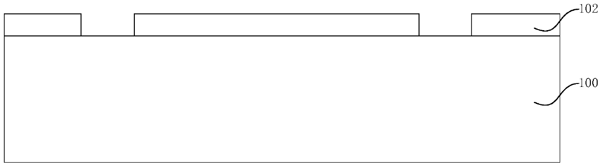
[0053] In step S01, a first substrate 100 is provided, the first substrate 100 includes an array storage area, an array common source doping area 110 is formed in the first substrate 100, and an insulating layer 110 is formed on the array storage area. A stacked layer 120 in which layers 122 and sacrificial layers 124 are alternately stacked, and memory cell strings 130 are formed in the stacked layer 120, refer to Figure 4 shown.

[0054] In the embodiment of the present application, the first substrate 100 is a semiconductor substrate, such as Si substrate, Ge substrate, SiGe substrate, SOI (Silicon On Insulator, Silicon On Insulator) or GOI...

Embodiment 2

[0083] In this embodiment, after the formation of stacked layers and the replacement of the gate layer, the array common source doping region is formed in the back process, and then the contact of the array common source doping region is formed from the back of the substrate, which is more conducive to the array common source doping region. Alignment of source doped regions and their contacts. The parts that are different from those in the first embodiment will be mainly described below, and the same parts will not be described again.

[0084] In step S201, a first substrate 100 is provided, and the first substrate 100 includes an array storage area, and stacked layers 120 in which insulating layers 122 and sacrificial layers 124 are alternately stacked are formed on the array storage area, and the stacked layers 120 is formed with memory cell string 130, refer to Figure 8 shown.

[0085] Different from step S101 in the first embodiment, in this embodiment, the array common...


PUM


Abstract

The invention provides a 3D NAND storage device and a manufacturing method thereof. After a stacked layer is formed, a sacrificial layer in the stacked layer is replaced with a gate layer by a gate line slit, secondly, a dielectric material is filled in the gate line slit, and an array co-source doped region is extracted from a back side of a substrate. The dielectric material is filled in the gate line slit, common source contact is formed on the back side of the substrate, a parasitic capacitor between the gate line slit and a word line is eliminated, breakdown between the word line and the common source contact is avoided, and device performance is improved.

Description

technical field [0001] The invention relates to the field of semiconductor devices and manufacturing thereof, in particular to a 3D NAND storage device and a manufacturing method thereof. Background technique [0002] NAND storage devices are non-volatile storage products with low power consumption, light weight and good performance, and are widely used in electronic products. [0003] Planar NAND devices are close to the limit of practical expansion. In order to further increase storage capacity and reduce storage cost per bit, 3D NAND storage devices are proposed. In the structure of 3D NAND storage devices, the method of vertically stacking multi-layer gates is adopted. The central area of ​​the stacked layer is an array storage area, and the edge area is a stepped structure. The array storage area is used to form a string of memory cells. The conductive layer in the stacked layer As the gate line of each layer of memory cells, the gate line is drawn out through the cont...

Claims


Application Information

Patent Timeline
Patent Type & Authority Applications(China)
IPC IPC(8): H01L27/11578
CPCH10B43/20
Inventor 吴继君袁刚
Owner YANGTZE MEMORY TECH CO LTD
Why Eureka
Try Eureka