Laser punching and cutting system for semiconductor materials

A laser drilling and cutting system technology, applied in laser welding equipment, welding/cutting auxiliary equipment, welding/welding/cutting items, etc., can solve the problem of low accuracy, influence of infrared ranging sensor measurement accuracy, and inconvenience of semiconductor drilling and other problems to achieve the effect of ensuring accuracy, simple structure and strong practicability

Active Publication Date: 2019-09-20
江苏守航实业有限公司
View PDF8 Cites 11 Cited by
  • Summary
  • Abstract
  • Description
  • Claims
  • Application Information

AI Technical Summary

Problems solved by technology

[0005] A laser drilling and cutting system for semiconductor materials proposed by the present invention solves the problem that when using a laser cutting device to process semiconductors, the infrared ranging sensor is generally placed in the outside world for distance measurement, which will cause The generated waste affects the measurement accuracy of the infrared distance measuring sensor. In addition, in the prior art, the X / Y axis drives the laser cutting device to move, which is very inconvenient when drilling semiconductors, and the accuracy of drilling into a circle is also low. not high problem

Method used


Image

  • Laser punching and cutting system for semiconductor materials
  • Laser punching and cutting system for semiconductor materials
  • Laser punching and cutting system for semiconductor materials

Examples


Embodiment Construction

[0020] The following will clearly and completely describe the technical solutions in the embodiments of the present invention with reference to the accompanying drawings in the embodiments of the present invention. Obviously, the described embodiments are only some, not all, embodiments of the present invention.

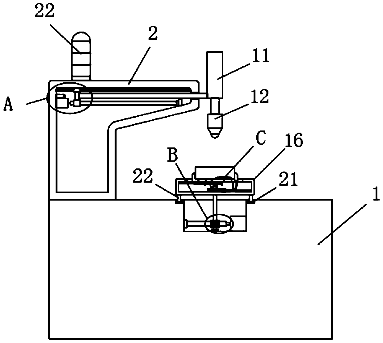
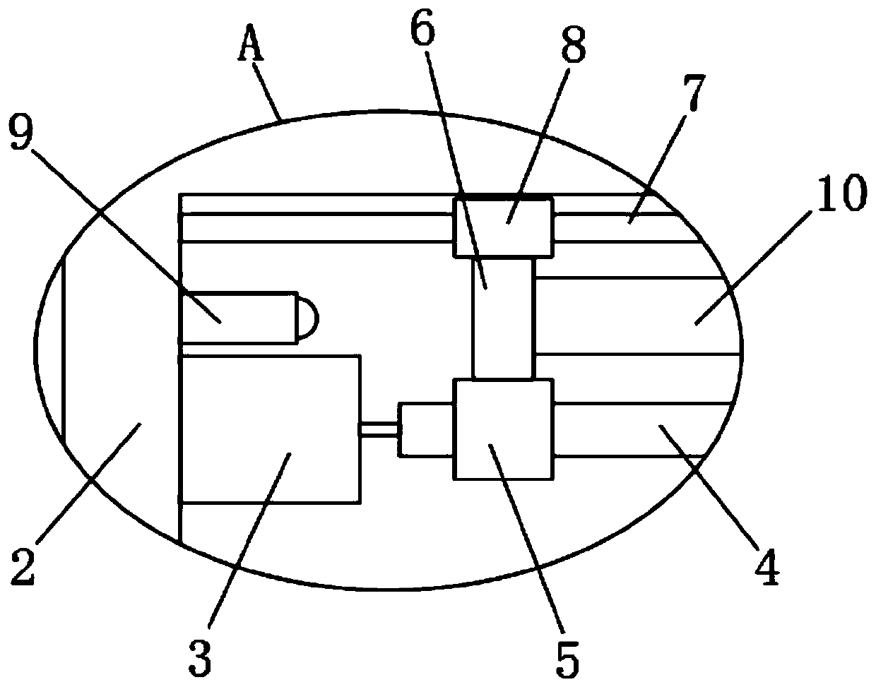
[0021] refer to Figure 1-4 , a laser drilling and cutting system for semiconductor materials, comprising a base 1, the upper side wall of the base 1 is fixedly connected with a mounting seat 2, the upper end side wall of the mounting seat 2 is fixedly connected with a multi-color warning light 22, and the multi-color warning light Lamp 22 adopts red, yellow and green. When green, it shows that the work is safe. When it is red and yellow, it shows that there is a mistake in the punching process, and reminds the workers to carry out maintenance. The multi-color warning lights 22 are electrically connected with the infrared ranging sensor 9 and the servo motor respectiv...


PUM


Abstract

The invention belongs to the field of semiconductors, and particularly relates to a laser punching and cutting system for semiconductor materials. Aiming at the problems that waste produced by existing cutting are splashed to influence the accuracy of an infrared distance measurement sensor, and the punching operation cannot be carried out conveniently by utilizing an X/Y axis, the invention provides the following scheme that the laser punching and cutting system for the semiconductor materials comprises a base, wherein an installation seat is fixedly connected to the upper end side wall of the base and is of a hollow structure; a stepping motor is fixedly connected to the inner wall of the installation seat; a ball screw matched with an output shaft of the stepping motor is rotatably connected to the inner wall of the installation seat; a sliding block is slidably arranged on the ball screw in a sleeving way; a light barrier is fixedly connected to the upper end side wall of the sliding block; and a sliding rod is fixedly connected between two side inner walls of the installation seat. The infrared distance measurement sensor measures the light barrier under the protection of the installation seat, so that the extraneous interference is reduced, and the distance measurement accuracy is improved; and through the cooperation of a worm and a worm wheel, a working table rotates so as to quickly accomplishing punching and cutting.

Description

technical field [0001] The invention relates to the technical field of semiconductor processing, in particular to a laser drilling and cutting system for semiconductor materials. Background technique [0002] A semiconductor refers to a material whose conductivity at room temperature is between that of a conductor and an insulator. Semiconductors have a wide range of applications in radios, televisions, and temperature measurement. For example, a diode is a device made of a semiconductor. A semiconductor is a material whose electrical conductivity can be controlled, ranging from an insulator to a conductor. No matter from the perspective of technology or economic development, the importance of semiconductors is enormous. The core units of most of today's electronic products, such as computers, mobile phones or digital recorders, are closely related to semiconductors. Common semiconductor materials include silicon, germanium, gallium arsenide, etc., and silicon is the mos...

Claims


Application Information

Patent Timeline
Patent Type & Authority Applications(China)
IPC IPC(8): B23K26/38B23K26/36B23K26/70B23K37/04
CPCB23K26/36B23K26/38B23K37/04B23K26/702B23K2103/56
Inventor 魏守冲
Owner 江苏守航实业有限公司
Why Eureka
Try Eureka