Transfer substrate, transfer method of light-emitting diode and transfer equipment

A technology for light-emitting diodes and substrates, which is used in semiconductor/solid-state device testing/measurement, semiconductor devices, electrical components, etc., and can solve the problems of difficult removal of Micro-LEDs and easy damage to array substrates.

Active Publication Date: 2019-09-20
SHANGHAI TIANMA MICRO ELECTRONICS CO LTD
View PDF10 Cites 8 Cited by
  • Summary
  • Abstract
  • Description
  • Claims
  • Application Information

AI Technical Summary

Problems solved by technology

[0005] Embodiments of the present invention provide a transfer substrate, a transfer method for light-emitting diodes, and transfer equipment to solve the problem in the prior art that during the transfer process of Micro-LEDs, it is difficult to remove the abnormally luminous Micro-LEDs, and the use of laser The problem that cutting is easy to damage the array substrate

Method used


Image

  • Transfer substrate, transfer method of light-emitting diode and transfer equipment
  • Transfer substrate, transfer method of light-emitting diode and transfer equipment
  • Transfer substrate, transfer method of light-emitting diode and transfer equipment

Examples


Embodiment Construction

[0053] Aiming at the problems existing in the prior art that during the Micro-LED transfer process, the abnormally luminous Micro-LED is difficult to remove, and the array substrate is easily damaged by laser cutting, the embodiment of the present invention provides a transfer substrate and a light-emitting diode. Transfer methods and transfer equipment.

[0054] The specific implementations of the transfer substrate, light-emitting diode transfer method and transfer equipment provided by the embodiments of the present invention will be described in detail below with reference to the accompanying drawings. The size and shape of each structure in the drawings do not reflect the real scale, but are only intended to schematically illustrate the content of the present invention.

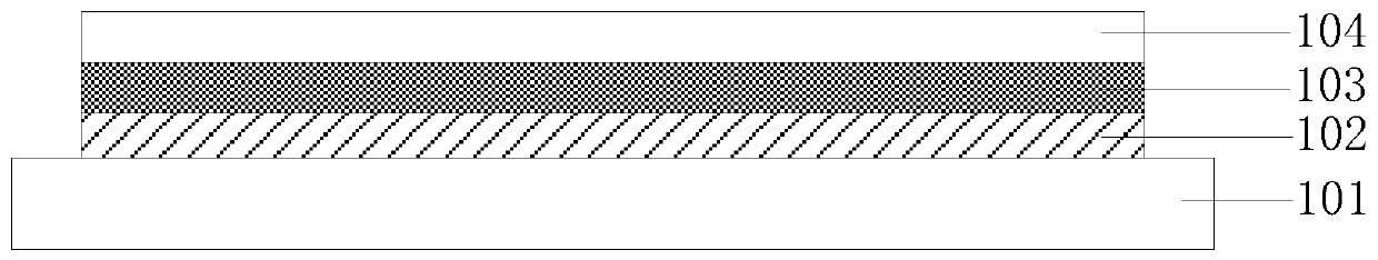
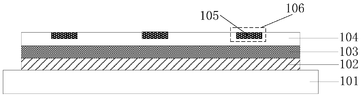
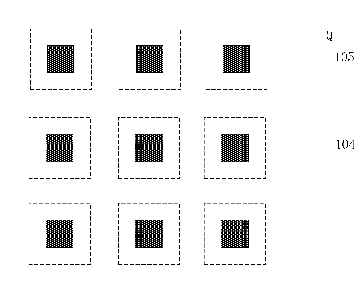
[0055] In the first aspect, the embodiment of the present invention provides a transport substrate, such as figure 1 As shown, it includes: a substrate 101, a reflective layer 102 located on the side of...


PUM


Abstract

The invention discloses a transfer substrate, a transfer method of a light-emitting diode and transfer equipment. The transfer substrate comprises a substrate, a reflecting layer, an optical conversion layer and a light-sensitive visbreaking film, wherein the reflecting layer is arranged at one side of the substrate, the optical conversion layer is arranged at one side, deviating from the substrate, of the reflecting layer, the light-sensitive visbreaking film is arranged at one side, deviating from the reflecting layer, of the optical conversion layer, the optical conversion layer is used for converting a light ray within a certain wavelength range to non-visible light, the light-sensitive visbreaking film is used for pasting the light-emitting diode, and the viscosity is reduced to relieve the light-emitting diode after irradiation of the non-visible light. By the transfer substrate, the transferring and the detection of the light-emitting diode can be simultaneously completed, the light-emitting diode with abnormal in light emitting is found out and transferred before a binding process, the problems that the light-emitting diode with abnormal light emitting is difficult to take out and the array substrate is damaged by a laser cutting process are prevented, the transfer process flow is simplified, and the transfer yield and efficiency is improved; and moreover, a light source of the non-visible light is not needed to be additionally arranged, and the transfer substrate is simple in structure and relatively low in detection cost.

Description

technical field [0001] The invention relates to the field of display technology, in particular to a method and equipment for transferring substrates and light-emitting diodes. Background technique [0002] With the development of light emitting diode (Light Emitting Diode, LED), micro light emitting diode (Micro-LED) display technology has become one of the hotspots of future display technology. control, high luminance, low power consumption, ultra-high resolution and high chromaticity, etc., but there are many technical difficulties in Micro-LED display technology, especially the mass transfer technology. [0003] The process of transferring Micro-LEDs is generally as follows: transfer Micro-LEDs to the array substrate, bind the electrodes of Micro-LEDs to the array substrate, control the light emission of Micro-LEDs for lighting detection, and use The laser cuts off the electrical connection between the electrode of the Micro-LED and the array substrate, thereby removing ...

Claims


Application Information

Patent Timeline
IPC IPC(8): H01L21/683H01L21/66H01L33/48
CPCH01L21/6835H01L21/6836H01L22/20H01L33/48H01L2221/68368H01L2221/68381
Inventor 符鞠建
Owner SHANGHAI TIANMA MICRO ELECTRONICS CO LTD
Why Eureka
Try Eureka