Circularly polarized laser source coupling microcavity
A laser light source, coupled microcavity technology, used in optics, nonlinear optics, instruments, etc., can solve the problem of inability to achieve gain amplification, and achieve the requirements of enhancing Faraday rotation effect, enhancing interaction, gain and loss parameters. Effect
- Summary
- Abstract
- Description
- Claims
- Application Information
AI Technical Summary
Problems solved by technology
Method used
Image
Examples
Embodiment 1
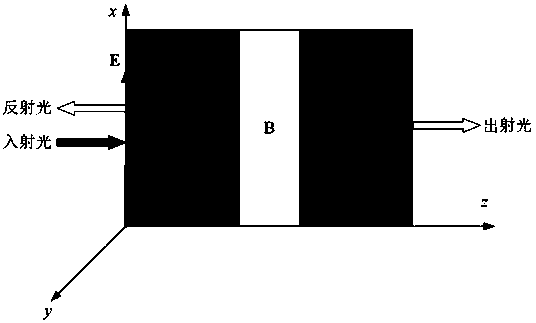
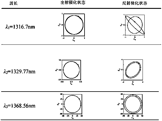
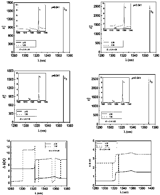
[0023] A circularly polarized laser light source coupling microcavity is a one-dimensional layered structure distributed along the z axis and extending in the xoy plane. The microcavity is formed by coupling the ABCD layers with each other, and the structure is expressed as DADBDCD, where the D layer It is a metal material, A layer and C layer are electromagnetic wave gain and electromagnetic wave loss materials respectively, and B layer is a defect layer composed of magneto-optical materials. The thickness of each layer: the thickness of A and C is 400nm, the thickness of B layer is 800nm, and the thickness of D layer is 205nm. The metal material layer is silver, and its effective metal plasma frequency is 4×10 15 S -1 . The electromagnetic wave gain material is a neodymium alumina laser gain material, which is produced by dissolving high-concentration neodymium ions into alumina crystals. The electromagnetic wave loss material is graphene. The magneto-optic material is a...
Embodiment 2
[0025]A circularly polarized laser light source coupling microcavity is a one-dimensional layered structure distributed along the z axis and extending in the xoy plane. The microcavity is formed by coupling the ABCD layers with each other, and the structure is expressed as DADBDCD, where the D layer It is a metal material, A layer and C layer are electromagnetic wave gain and electromagnetic wave loss materials respectively, and B layer is a defect layer composed of magneto-optical materials. The thickness of each layer: the thickness of A and C is 400nm, the thickness of B layer is 800nm, and the thickness of D layer is 205nm. The metal material layer is silver, and its effective metal plasma frequency is 4×10¹⁵S-1. The electromagnetic wave gain material is a neodymium alumina laser gain material, which is produced by dissolving high-concentration neodymium ions into alumina crystals. The electromagnetic wave loss material is graphene. The magneto-optical material is a rare...
Embodiment 3
[0027] An elliptically polarized laser light source coupling microcavity is a one-dimensional layered structure distributed along the z axis and extending in the xoy plane. The microcavity is formed by coupling the ABCD layers with each other, and the structure is expressed as DADBDCD, where the D layer It is a metal material, A layer and C layer are electromagnetic wave gain and electromagnetic wave loss materials respectively, and B layer is a defect layer composed of magneto-optical materials. The thickness of each layer: the thickness of A and C is 400nm, the thickness of B layer is 800nm, and the thickness of D layer is 205nm. The metal material layer is silver, and its effective metal plasma frequency is 4×10¹⁵S -1 . The electromagnetic wave gain material is a neodymium alumina laser gain material, which is produced by dissolving high-concentration neodymium ions into alumina crystals. The electromagnetic wave loss material is graphene. The magneto-optical material is...
PUM
| Property | Measurement | Unit |
|---|---|---|
| thickness | aaaaa | aaaaa |
| thickness | aaaaa | aaaaa |
| thickness | aaaaa | aaaaa |
Abstract
Description
Claims
Application Information


