Silicon micro-nano structure-based photovoltaic device and preparation method and application thereof

A nano-structure and silicon-micro technology, applied in the field of silicon micro-nano structure-based hydrovoltaic devices and its preparation, can solve the problems of low output power and restrictions on commercial applications, and achieve high current density, excellent power output, and high sensitivity Effect

Inactive Publication Date: 2019-09-27
SUZHOU UNIV
View PDF9 Cites 7 Cited by
  • Summary
  • Abstract
  • Description
  • Claims
  • Application Information

AI Technical Summary

Problems solved by technology

After several years of development, hydrovoltaic technology covers a wide range of material systems based on nano-carbon materials, including insulators and semiconductors, but is limited by low output power, which also seriously restricts its commercial application.

Method used


Image

  • Silicon micro-nano structure-based photovoltaic device and preparation method and application thereof
  • Silicon micro-nano structure-based photovoltaic device and preparation method and application thereof
  • Silicon micro-nano structure-based photovoltaic device and preparation method and application thereof

Examples


Embodiment 1

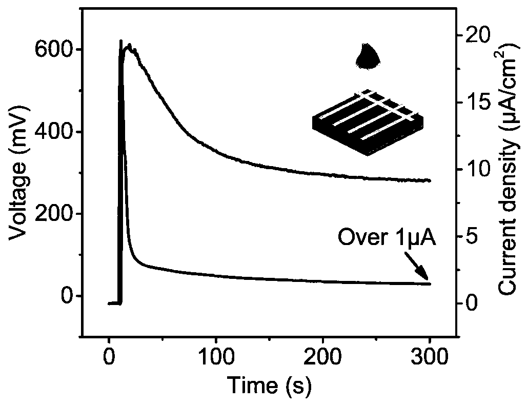
[0030] Example 1: Preparation of silicon nanowire array hydrovoltaic device

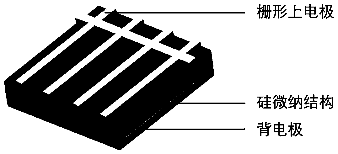
[0031] The structure of the hydroelectric device based on the silicon micro-nano structure in the present invention includes a gate-shaped upper electrode, a silicon nano-micro-nano structure, and a back electrode. Taking a silicon nanowire array-based hydrovoltaic device as an example, its preparation method includes the following steps:

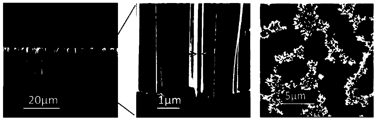
[0032] (1) Silicon wafers with different doping concentrations undergo metal-assisted chemical etching, and silicon nanowire arrays with uniform morphology and adjustable length can be obtained by adjusting the concentration of etching solution and etching temperature.

[0033] (2) By means of the film-forming process, a fully-covered silver gel electrode is prepared on the back of the silicon nanowire array, and a grid-shaped silver gel electrode is prepared on the front of the silicon nanowire array by printing.

[0034] (3) After the silver glue dries naturall...


PUM


Abstract

The invention discloses a preparation method of a silicon micro-nano structure-based photovoltaic device, which comprises the following steps: S1, providing a doped silicon wafer, and etching on the front surface of the silicon wafer by adopting a metal-assisted etching method to form a silicon micro-nano structure; S2, covering a back electrode, which is a metal electrode or a conductive polymer electrode, on the back surface of the silicon wafer through a film forming process or a physical vapor deposition method; and S3, printing a grid electrode on the surface of the silicon micro-nano structure to obtain the photovoltaic device. The invention also provides a silicon micro-nano structure-based photovoltaic device prepared by the method and an application thereof. The silicon micro-nano structure-based photovoltaic device is simple and safe in preparation process, has excellent power output and relatively high current density, has high sensitivity to moisture, and has a wide practical application prospect in the technical fields of humidity sensors and novel energy conversion.

Description

technical field [0001] The invention relates to the field of hydrovolt technology, in particular to a hydrovolt device based on silicon micro-nano structure and its preparation method and application. Background technique [0002] In today's society, energy and environmental issues are increasingly affecting the rapid development of society. The research and application of clean and renewable energy has aroused widespread concern in society. More and more forms of renewable energy collection are competing to develop, such as nano friction power generation technology, piezoelectric technology, thermoelectric technology and so on. [0003] Recently, as a new type of energy conversion technology, hydrovoltaic technology has shown rapid development momentum. As a technology to generate electric energy by means of the flow of water, it has broad application prospects because of its convenient and easy-to-obtain, low-cost, non-toxic, non-polluting and other excellent properties....

Claims


Application Information

Patent Timeline
IPC IPC(8): B81B3/00
CPCB81B3/0018B81B3/0027
Inventor 孙宝全秦元帅宋涛
Owner SUZHOU UNIV
Why Eureka
Try Eureka