Methane gas sensor on basis of organic thin film transistor and preparation method of methane gas sensor
A technology of thin-film transistors and methane gas, which is applied in instruments, scientific instruments, measuring devices, etc., can solve the problems of easy interference of response signals, poor stability of measured values, high cost consumption, etc., and achieve simplified device preparation process, large response current, The effect of good electrical characteristics
- Summary
- Abstract
- Description
- Claims
- Application Information
AI Technical Summary
Problems solved by technology
Method used
Image
Examples
Embodiment 1
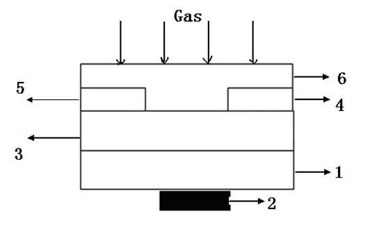
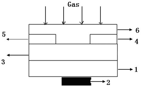
[0040] The organic thin film transistor gas sensor is composed of a glass substrate, a gate electrode, a gate insulating layer, a drain electrode, a source electrode, and an organic layer. On top of the electrode insulating layer, an organic layer connects the source electrode and the drain electrode. The organic layer is made of p-type organic semiconductor material pentacene.
[0041]Clean the glass substrate on which the gate electrode ITO has been sputtered. Firstly, after scrubbing with a cleaning agent, the cleaning agent solution is ultrasonicated for 10 minutes, then the substrate is scrubbed with a detergent, rinsed with deionized water, and the deionized aqueous solution is ultrasonicated for 10 minutes. Sonicate in acetone solution for 10 minutes, and finally in ethanol solution for 10 minutes. After cleaning, dry the substrate with nitrogen; set the front rotation to 500 rpm and the back rotation to 1000 rpm to spin coat the insulating layer PMMA with a thic...
Embodiment 2
[0044] Clean the glass substrate on which the gate electrode ITO has been sputtered. Firstly, after scrubbing with a cleaning agent, the cleaning agent solution is ultrasonicated for 10 minutes, then the substrate is scrubbed with a detergent, rinsed with deionized water, and the deionized aqueous solution is ultrasonicated for 10 minutes. Sonicate in acetone solution for 10 minutes, and finally in ethanol solution for 10 minutes. After cleaning, dry the substrate with nitrogen; set the front rotation to 500 rpm and the back rotation to 1000 rpm to spin-coat the insulating layer PS with a thickness of 20 nanometers; then anneal at 150°C for 1 hour; Then use the vacuum evaporation method to evaporate the source electrode and the drain electrode. The source and drain electrodes are both Au electrodes. -0.02 nanometers / second, the thickness reaches 25 nanometers; the gas sensor is obtained.
Embodiment 3
[0046] Clean the glass substrate on which the gate electrode ITO has been sputtered. First, after scrubbing with a cleaning agent, the cleaning agent solution is ultrasonicated for 15 minutes, then the substrate is scrubbed with a detergent, rinsed with deionized water, and the deionized aqueous solution is ultrasonicated for 15 minutes. Sonicate in acetone solution for 15 minutes, and finally in ethanol solution for 15 minutes. After cleaning, dry the substrate with nitrogen; set the front rotation to 500 rpm and the back rotation to 1000 rpm to spin-coat the insulating layer of PVA with a thickness of 2000 nanometers; then anneal at 150 ° C for 1 hour; Then use the vacuum evaporation method to evaporate the source electrode and the drain electrode. The source and drain electrodes are both Au electrodes. -0.02 nanometers / second, the thickness reaches 25 nanometers; the gas sensor is obtained.
PUM
| Property | Measurement | Unit |
|---|---|---|
| Thickness | aaaaa | aaaaa |
| Thickness | aaaaa | aaaaa |
| Thickness | aaaaa | aaaaa |
Abstract
Description
Claims
Application Information


