Organic electroluminescent device with novel structure and method for fabricating the same

An electroluminescence and device technology, applied in the field of organic electroluminescence devices, can solve problems such as low device efficiency, and achieve the effects of increasing proportion, improving work function and good reproducibility

Inactive Publication Date: 2008-02-27
TIANJIN UNIVERSITY OF TECHNOLOGY
View PDF0 Cites 9 Cited by
  • Summary
  • Abstract
  • Description
  • Claims
  • Application Information

AI Technical Summary

Problems solved by technology

[0005] The purpose of the present invention is to solve the problem of low efficiency of the existing organic electroluminescent devices due to the unbalanced injection and transport of electrons and holes, and provides a metal thin film modified by a self-assembled monomolecular film Preparation method of organic electroluminescent device with hole injection buffer layer

Method used


Image

  • Organic electroluminescent device with novel structure and method for fabricating the same

Examples


Embodiment 1

[0031] (1) After repeatedly cleaning the 3mm×3mm ITO glass in detergent, soak it in isopropanol, acetone and chloroform solution respectively and ultrasonically clean it, and finally dry it in an infrared oven for use;

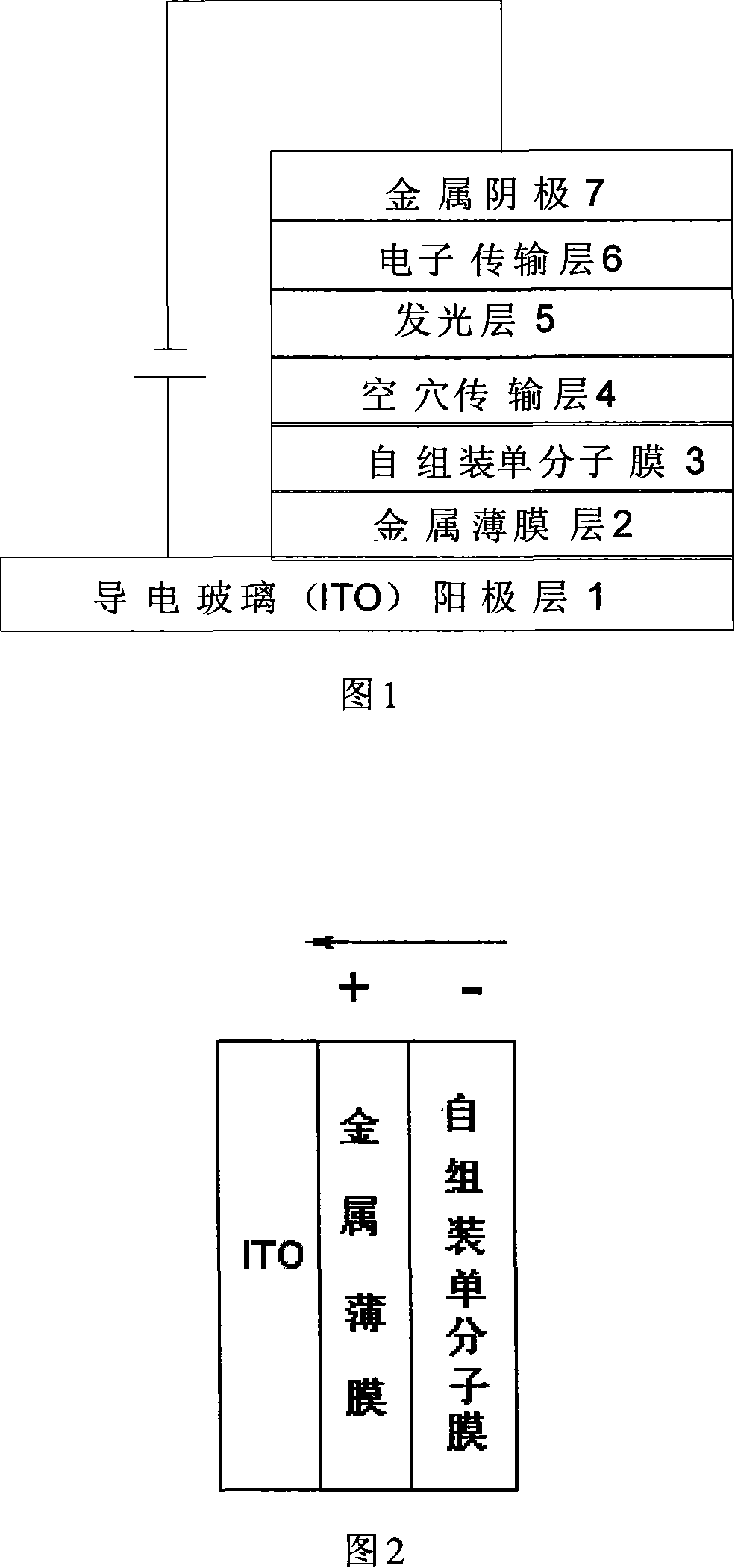
[0032] (2) A 12 nm-thick Ag film was evaporated on the surface of the above-mentioned cleaned ITO glass by a vacuum evaporation method.

[0033] (3) Put the above-mentioned ITO glass coated with a 12nm thick Ag film into a concentration of 1×10 -3 mol / L of 3-trifluoromethylbenzyl mercaptan in absolute ethanol solution for 0.5h, take it out, and wash it with absolute ethanol for 3 times. Blow dry with nitrogen stream.

[0034] (4) PVK and TPD were mixed at a mass ratio of 1:1 to 1::2, and dissolved in chloroform to prepare a solution with a concentration of 2 mg / ml. Films were formed on ITO glass by spin coating. Film-forming conditions: low speed 1000-1500rpm, film-forming time about 20s; high-speed 3000-4000rpm, film-forming time about 30s, after completio...

Embodiment 2

[0040] A 12nm thick Ag film was evaporated on the cleaned ITO glass surface by vacuum evaporation method. Put the above-mentioned ITO glass coated with Ag film into the concentration of 1×10 -3 mol / L 4-fluorobenzenethiol in absolute ethanol solution for 0.5h and then taken out. Wash 3 times with absolute ethanol and blow dry with nitrogen flow. 15nm m-MTDATA, 15nm NPB, and 60nm Alq were sequentially deposited by vacuum evaporation method 3 , 1nm LiF and 100nm Al, stable electroluminescence can be obtained between 3.5 and 13.5V. The highest brightness is 13560cd / m at 13.5V 2 ; The maximum luminous efficiency at 13V is 4.3cd / A. The contrast device has a maximum brightness of 10000cd / m at 13.5V 2 , and the corresponding luminous efficiency is 2.4cd / A.


PUM

PropertyMeasurementUnit
Thicknessaaaaaaaaaa
Thicknessaaaaaaaaaa
Luminous efficiencyaaaaaaaaaa

Abstract

This inventive electroluminescent component involves successively: an electroconductive glass ITO anode layer; a metal thin film layer modified by self-package monomolecular film used as hole-injection buffer layer; a hole-transmission layer; a light-emitting layer; an electron transmission layer and a metal cathode layer. In this invention, due to the use of organic molecule self-package technique, the self-package single-molecular deposited onto metal film on anode surface which forms self-dipole film as the hole-injection buffer-layer, so it can obviously control the injection of the hole-carrier into hole-transmission layer, to achieve the balance between hole and electron-injection in the light-emitting layer, to improve the brightness and light-emitting efficiency of the component.

Description

【Technical field】: [0001] The invention relates to an organic electroluminescent device using a metal thin film modified by a self-assembled monomolecular film as a hole injection buffer layer, and belongs to the technical field of organic electroluminescence. In particular, it relates to a method of using the dipolarity of self-assembled molecules to control the injection of hole carriers into the hole transport layer, so as to realize the balanced injection of holes and electrons in the light-emitting layer, thereby improving the luminous efficiency and brightness of the device. 【Background technique】: [0002] In the 21st century of information explosion, flat panel display technology as an information carrier will dominate the field of information display. As a new force in the field of display technology, organic electroluminescent devices (OLEDs) involve different disciplines such as materials science, luminescence optics and microelectronics, and have outstanding perf...

Claims


Application Information

Patent Timeline
IPC IPC(8): H01L51/50H01L51/52H01L51/54H01L51/56
Inventor 杨利营印寿根陈向舟许昊叶丹琴华玉林
Owner TIANJIN UNIVERSITY OF TECHNOLOGY
Why Eureka
Try Eureka