Method of forming 3D NAND memory

A 3DNAND, memory technology, applied in the direction of electric solid devices, semiconductor devices, electrical components, etc., can solve the problem of easy inclination of gate spacers, short circuit between gate spacers and channel through holes, etc.

Active Publication Date: 2019-09-27
YANGTZE MEMORY TECH CO LTD
View PDF4 Cites 6 Cited by
  • Summary
  • Abstract
  • Description
  • Claims
  • Application Information

AI Technical Summary

Problems solved by technology

[0004] Existing memories generally include several memory blocks (Blocks), and the memory blocks are generally separated by Gate Line Slits (GLS) vertically penetrating the stacked struc

Method used


Image

  • Method of forming 3D NAND memory
  • Method of forming 3D NAND memory
  • Method of forming 3D NAND memory

Examples


no. 1 example 3D

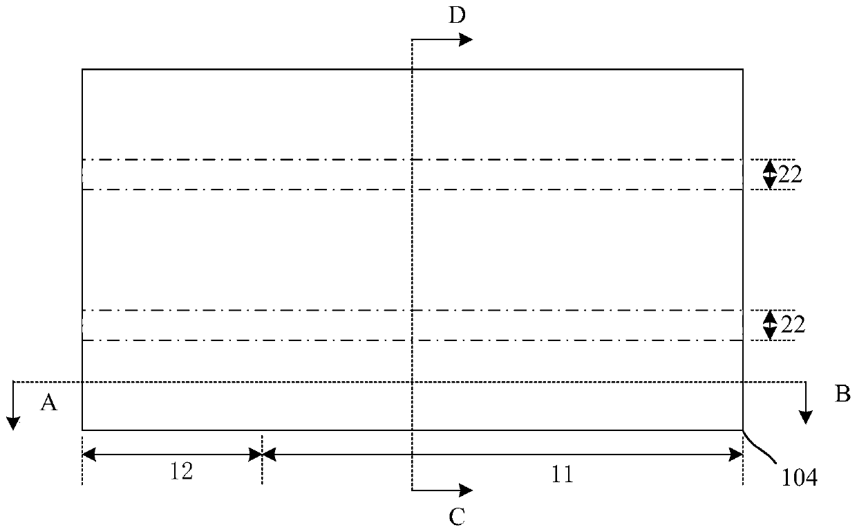
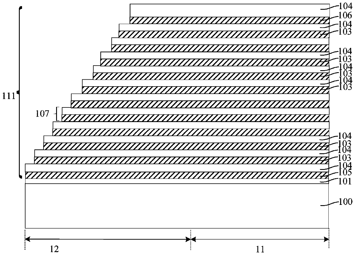
[0039] Figure 1-Figure 14 It is a structural schematic diagram of the 3D NAND formation process according to the first embodiment of the present invention.

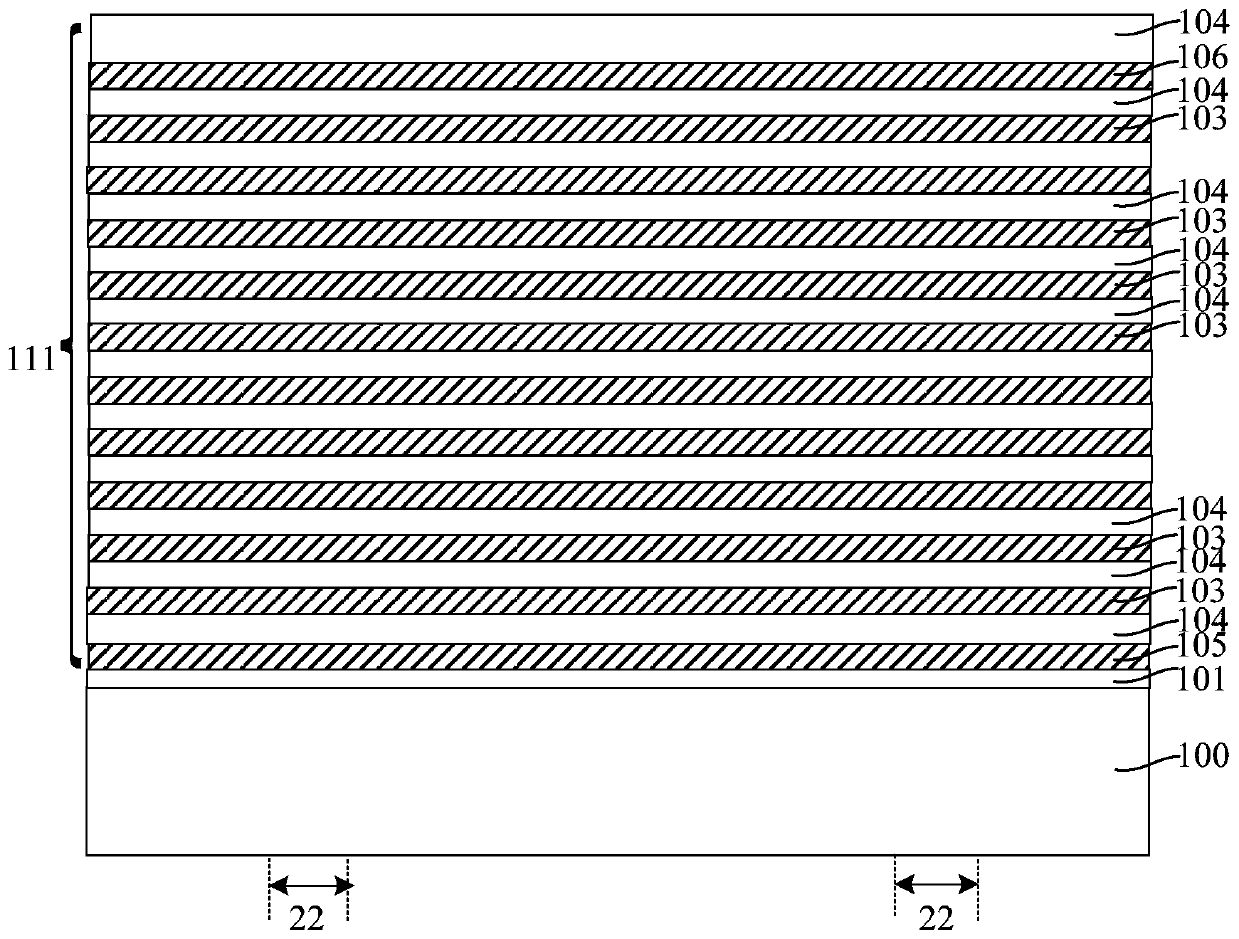
[0040] refer to figure 1 and figure 2 , figure 2 for figure 1 A schematic diagram of a cross-sectional structure along a cutting line CD provides a semiconductor substrate 100 on which a stacked structure 111 in which sacrificial layers 103 and isolation layers 104 are alternately stacked is formed.

[0041] The material of the semiconductor substrate 100 can be single crystal silicon (Si), single crystal germanium (Ge), or silicon germanium (GeSi), silicon carbide (SiC); it can also be silicon on insulator (SOI), germanium on insulator (GOI); or other materials, such as III-V group compounds such as gallium arsenide. In this embodiment, the material of the semiconductor substrate 100 is single crystal silicon (Si).

[0042] The stacked structure 111 includes several alternately stacked sacrificial layers 103 an...


PUM


Abstract

The invention provides a method of forming a 3D NAND memory, and the method comprises the steps: etching a stacking structure to form a plurality of grid separation grooves penetrating through the stacking structure, and then forming filling layers in the grid separation grooves, wherein the grid separation grooves are filled with the filling layers; after the filling layer is formed, etching the stacking structures at the two sides of the gate isolation grooves to form a plurality of channel through holes penetrating through the stacking structures; forming a storage structure in the channel through hole; after the storage structure is formed, removing the filling layer, and exposing the gate isolation groove; removing a sacrificial layer, and correspondingly forming a control gate at a position where the sacrificial layer is removed; and forming an array common source in the gate isolation groove. In the invention, because the step of forming the gate isolation groove is executed before the step of forming the channel through hole and the step of forming the storage structure in the channel through hole, the gate isolation grooves do not incline, thereby preventing the gate isolation grooves and the channel through hole from being short-circuited.

Description

technical field [0001] The invention relates to the field of semiconductor manufacturing, in particular to a method for reducing 3D NAND memory. Background technique [0002] NAND flash memory is a non-volatile storage product with low power consumption, light weight and good performance, and has been widely used in electronic products. At present, the NAND flash memory with a planar structure is close to the limit of practical expansion. In order to further increase the storage capacity and reduce the storage cost per bit, a 3D NAND memory with a 3D structure is proposed. [0003] The formation process of the existing 3D NAND memory generally includes: forming a stacked structure in which isolation layers and sacrificial layers are alternately stacked on the substrate; etching the stacked structure, forming channel vias in the stacked structure, and forming channel vias Finally, etch the substrate at the bottom of the channel via hole to form a groove in the substrate; in ...

Claims


Application Information

Patent Timeline
IPC IPC(8): H01L27/1157H01L27/11582
CPCH10B43/35H10B43/27
Inventor 王香凝耿静静王攀张慧刘新鑫吴佳佳肖梦
Owner YANGTZE MEMORY TECH CO LTD
Why Eureka
Try Eureka