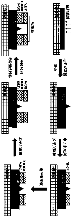
Vertical type nano gap vacuum transistor with extended gate structure and preparation method thereof
A gate structure, vertical technology, applied in the field of vertical nano-gap vacuum transistors and its preparation, can solve the problems of miniaturization, light weight and integration, bulky and bloated vacuum electronic systems, etc., and improve emission efficiency And the effects of current density, enhanced surface electric field strength, and reduced gate leakage current
- Summary
- Abstract
- Description
- Claims
- Application Information
AI Technical Summary
Problems solved by technology
Method used
Image
Examples
Embodiment 1
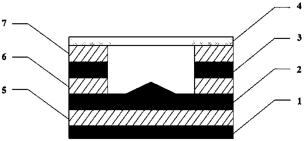
[0047] figure 2 It is a schematic cross-sectional view of an extended gate structure in the present invention, including a back gate 1 , an emitter 2 , an extended gate 3 , a collector 4 and oxide insulating substrates 5 , 6 and 7 . The oxide substrate 5 is arranged between the back gate 1 and the emitter 2, the oxide substrate 6 is arranged between the emitter 2 and the extension gate 3, and the oxide substrate 7 is arranged on the extension Both the gate 3 and the collector 4 are used to isolate the leakage current between the electrodes; the distance between the emitter 2 and the collector 4 is on the scale of sub-100 nanometers.
Embodiment 2
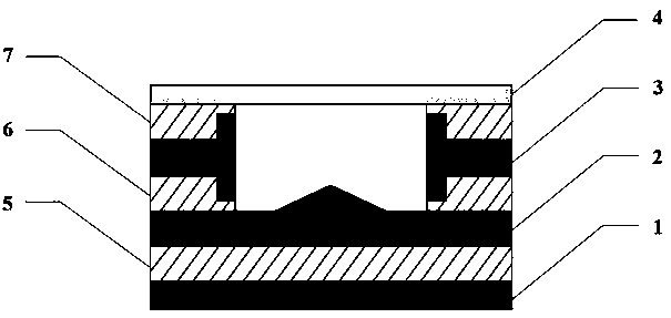
[0049] image 3 It is a schematic cross-sectional view of a T-shaped extended gate structure in the present invention, increasing the area opposite the gate to the emitter, thereby effectively increasing the electric field intensity on the surface of the emitter, and improving the electron emission capability and current density of the device. It includes a back gate 1, an emitter 2, a T-shaped extended gate 3, a collector 4 and oxide insulating substrates 5, 6 and 7. The oxide substrate 5 is arranged between the back gate 1 and the emitter 2, the oxide substrate 6 is arranged between the emitter 2 and the T-shaped extended gate 3, and the oxide substrate 7 is arranged Between the T-shaped extended gate 3 and the collector 4, both are used to isolate the leakage current between the electrodes; the distance between the emitter 2 and the collector 4 is on the scale of sub-100 nanometers.
PUM
| Property | Measurement | Unit |
|---|---|---|
| Thickness | aaaaa | aaaaa |
| Thickness | aaaaa | aaaaa |
Abstract
Description
Claims
Application Information


