Side anode vacuum channel nanogap triode and preparation method thereof

A nano-gap, triode technology, applied in cold cathode manufacturing, electrode system manufacturing, single discharge channel tube, etc., can solve the problems of difficult to achieve miniaturization, light weight and integration, bulky and bloated vacuum electronic systems, etc. Requirements and application scope of vacuum degree, breakthrough of technical bottleneck, effect of reducing leakage current

Pending Publication Date: 2021-12-14
SOUTHEAST UNIV
View PDF0 Cites 0 Cited by
  • Summary
  • Abstract
  • Description
  • Claims
  • Application Information

AI Technical Summary

Problems solved by technology

However, limited by complex mechanical processing and other reasons, traditional vacuum electronic systems are often bulky and bloated, making it difficult to achieve miniaturization, light weight and integration

Method used


Image

  • Side anode vacuum channel nanogap triode and preparation method thereof
  • Side anode vacuum channel nanogap triode and preparation method thereof
  • Side anode vacuum channel nanogap triode and preparation method thereof

Examples


Embodiment 1

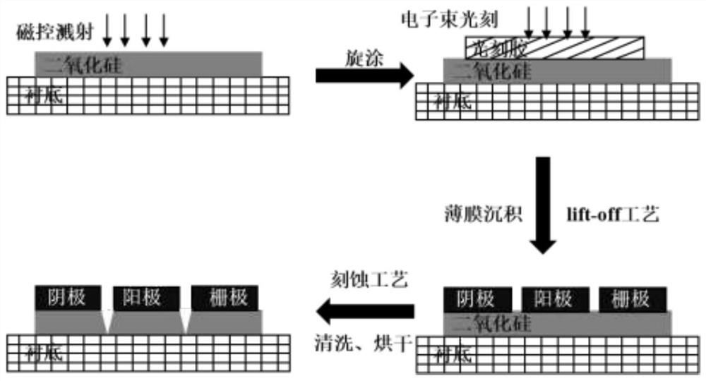
[0049] figure 2 A schematic flow chart of the preparation process of the vacuum channel nanogap triode in the present invention is shown. Take the cathode 2, anode 3 and gate 5 as an example of metal or semiconductor materials: first, the silicon wafer is ultrasonically cleaned with acetone, isopropanol and deionized water in sequence, and the surface is dried with nitrogen; magnetron sputtering is used on the polished surface Spin-coat photoresist, and use electron beam lithography to expose a preset pattern area on the sample surface; after developing with a mixed solution of isopropanol and methyl isobutyl ketone, use chemical vapor phase deposition or electron beam evaporation and other thin film deposition processes to prepare semiconductor or metal thin films as cathode 2, anode 3 and grid 5; Ultrasonic cleaning in ionized water; finally, use wet or dry or focused ion beam etching and other etching processes to remove the nano-gap 3 and the surrounding substrate materi...

Embodiment 2

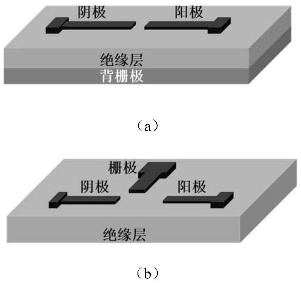
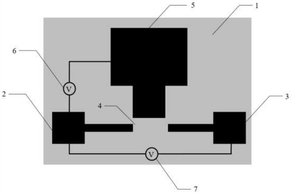
[0052] image 3 It is a plan view of the basic structure of the vacuum channel nano-gap triode in the present invention, and it is characterized in that: on the insulating base material 1, the cathode 2 and the grid 3 on the same straight line are made of conductive materials, and the cathode is connected to the anode and the grid. A gap 4 within 300 nanometers is kept between them, and an anode electrode 5 is arranged on one side of the gap region in the direction perpendicular to the straight line of the cathode and the grid. When the grid is applied with a modulation voltage 6 higher than that of the cathode, adjusting the grid modulation voltage can cause the cathode to emit electrons; setting a voltage 7 higher than the cathode on the anode and adjusting the anode voltage can make the electrons emitted by the cathode under the action of the anode voltage A part or all of them are hit on the anode, so as to form a nano-gap device triode structure with controllable current....

Embodiment 3

[0054] Figure 4 It is a top view of a V-type vacuum channel nano-gap triode in the present invention, and it is characterized in that: on the insulating base material 1, the cathode 2 and the grid 3 on the same straight line are made of conductive materials, and the cathode is connected to the anode, A V-shaped gap 4 within 300 nanometers is maintained between the gates, and an anode electrode 5 is arranged on one side of the gap region in a direction perpendicular to the straight line of the cathode and the grid. When the grid is applied with a modulation voltage 6 higher than that of the cathode, adjusting the grid modulation voltage can cause the cathode to emit electrons; setting a voltage 7 higher than the cathode on the anode and adjusting the anode voltage can make the electrons emitted by the cathode under the action of the anode voltage A part or all of them are hit on the anode, so as to form a nano-gap device triode structure with controllable current. The anode 5...


PUM


Abstract

The invention discloses a side anode vacuum channel nanogap triode and a preparation method thereof. The nanogap triode comprises a cathode, an anode, a grid electrode, and an oxide insulating layer; the nanogap means that the distance between the anode and the grid is kept within 300 nm; and the nanogap triode has similar electrical characteristics with a traditional field effect transistor, electrons are transported in a ballistic transport or tunneling mode in a vacuum channel, and the vacuum channel is smaller than / close to the average free path of the electrons in the air, the driving voltage is smaller than the first ionization potential of molecules, and the device can work normally without strict vacuum packaging. According to the structure, the technical bottleneck of a traditional electric vacuum device is simulated to be broken through, a miniaturized and integrated vacuum nano-electronic device is obtained by combining an existing semiconductor processing technology, the technical advantages of high frequency, quick response and no need of strict vacuum packaging are expected to be obtained, and the structure has high application potential in novel electronic components.

Description

technical field [0001] The invention relates to a side-anode vacuum channel nano-gap triode and a preparation method thereof, belonging to the field of novel vacuum micro-nano structures and field emission devices. Background technique [0002] Vacuum electronic devices have technical advantages such as high power, wide frequency bandwidth and high frequency, and are widely used in technical fields such as communication, radar, navigation and imaging. However, limited by complex machining and other reasons, traditional vacuum electronic systems are often bulky and bloated, making it difficult to achieve miniaturization, light weight and integration. The development of nanotechnology, whether it is advanced processing technology or the emergence of new nanomaterials, provides the possibility to break through the bottleneck of traditional vacuum electronic devices. In recent years, the emergence of nanogap structures has injected new vitality into vacuum nanoelectronic device...

Claims


Application Information

Patent Timeline
IPC IPC(8): H01J21/10H01J19/02H01J19/38H01J19/32H01J9/00
CPCH01J21/10H01J19/02H01J19/38H01J19/32H01J9/00
Inventor 张晓兵徐季史永佼雷威
Owner SOUTHEAST UNIV
Why Eureka
Try Eureka