Super-junction VDMOS device

A device and conductivity type technology, applied in the field of super-junction VDMOS devices, can solve the problems of super-junction MOSFET radiation effect and reinforcement research, VDMOS burnout, avalanche multiplication, etc., so as to reduce the probability of SEB, slow down the accumulation rate, The effect of reducing the current intensity

Pending Publication Date: 2019-10-08
UNIV OF ELECTRONICS SCI & TECH OF CHINA +1
View PDF0 Cites 6 Cited by
  • Summary
  • Abstract
  • Description
  • Claims
  • Application Information

AI Technical Summary

Problems solved by technology

Nuclear arrest causes lattice damage to the irradiated material, while electronic arrest causes ionization of the constituent atoms of the irradiated material, generating secondary electrons with hundreds of energies or higher, and along the track of the secondary electrons, a large number of If the current is large enough, it may cause the parasitic bipolar transistor in the VDMOS device to turn on. If the drain-source voltage reaches the breakdown voltage BVceo of the parasitic BJT, the collector area of ​​the parasitic BJT will occur The avalanche multiplies, forming a positive feedback, which eventually leads to the burning of VDMOS
[0004] In recent years, a lot of research has been done on the radiation effect and reinforcement of traditional power MOSFETs at home and abroad, and phased results have been achieved, but there are few reports on the radiation effects and reinforcement of super-junction MOSFETs so far.

Method used


Image

  • Super-junction VDMOS device
  • Super-junction VDMOS device

Examples


Embodiment 1

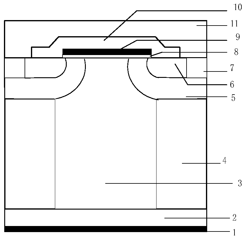
[0020]A super junction VDMOS device, comprising a first conductivity type heavily doped semiconductor substrate 2, a metallized drain electrode 1 located on the back of the first conductivity type heavily doped semiconductor substrate 2, a metallized drain electrode 1 located on the first conductivity type heavily doped semiconductor substrate The first conductivity type semiconductor column region 3 and the second conductivity type semiconductor column region 4 on the front surface of the substrate 2, the first conductivity type semiconductor column region 3 and the second conductivity type semiconductor column region 4 are arranged alternately, the second conductivity type semiconductor column region The top of 4 has a second conductivity type semiconductor base region 5, the side of the second conductivity type semiconductor base region 5 is in direct contact with the first conductivity type semiconductor column region 3, and the second conductivity type semiconductor base re...

Embodiment 2

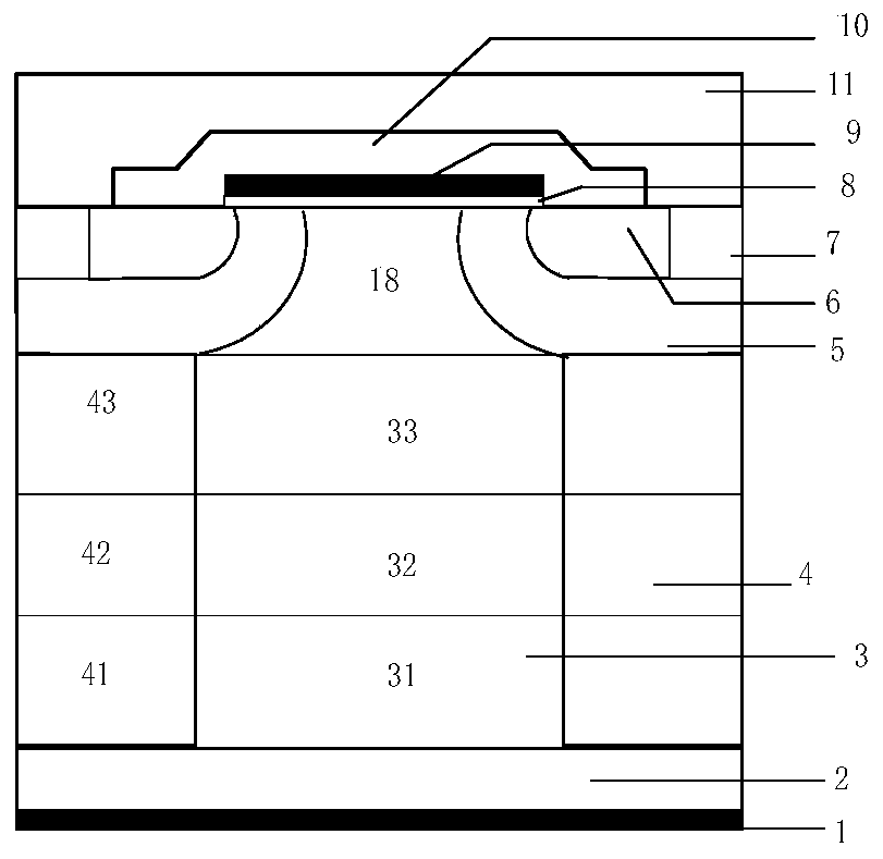
[0030] The difference between this embodiment and Embodiment 1 is: the first doped region 31 of the first conductivity type, the second doped region 32 of the first conductivity type, and the third doped region 33 of the first conductivity type. The impurity is non-uniformly distributed in this region, and the closer to the metallized drain side, the lower the doping concentration.

Embodiment 3

[0032] The difference between this embodiment and Embodiment 1 is: the first doped region 41 of the second conductivity type, the second doped region 42 of the second conductivity type, and the third doped region 43 of the second conductivity type. The impurity is non-uniformly distributed in this region, and the closer to the metallized drain side, the lower the doping concentration.


PUM


Abstract

The invention provides a super-junction VDMOS device comprising a first conductive type heavily doped semiconductor substrate, a metallized drain electrode, a first conductive type semiconductor column region and a second conductive type semiconductor column region. The first conductive type semiconductor column region and the second conductive type semiconductor column region are provided with three regions in which the doping concentration increases in sequence from bottom to top. The doping concentration of the P / N column uses a variable doping distribution which increases from bottom to top and the carrier lifetime of the JFET region is shortened by carrier lifetime control so that the current intensity flowing through the base region of the super-junction VDMOS uisng the structure canbe reduced, the conduction of the parasitic triodes inside the super-junction VDMOS can be effectively suppressed and the possibility of SEB of the device can be reduced. Meanwhile, the high doping concentration in the upper part of the P / N column forms a high barrier under the JFET region and the upper part of the P / N column so that the charge accumulation rate under the gate can be slowed downand the occurrence of SEGR can also be effectively suppressed through the carrier lifetime control of the JFET region.

Description

technical field [0001] The invention belongs to the technical field of power semiconductor devices, and relates to super junction VDMOS devices. Background technique [0002] At present, the application fields of power semiconductor devices are becoming wider and wider, and have become one of the foundations of modern industrial control and national defense equipment. Compared with bipolar transistors, vertical double-diffused metal oxide semiconductor field effect transistors (VDMOS) have the advantages of fast switching speed, low loss, high input impedance, low driving power, good frequency characteristics, and highly linear transconductance, so they become The most widely used new power device at present. However, when applied in the high-voltage field, VDMOS will have a so-called "silicon limit" bottleneck, that is, the increase in on-resistance with the withstand voltage will lead to a sharp increase in power consumption. As a representative of new power devices, sup...

Claims


Application Information

Patent Timeline
Patent Type & Authority Applications(China)
IPC IPC(8): H01L29/06H01L29/78
CPCH01L29/0684H01L29/7802
Inventor 任敏谭键文骆俊毅李泽宏张波
Owner UNIV OF ELECTRONICS SCI & TECH OF CHINA
Why Eureka
Try Eureka