Semiconductor structure and forming method thereof

A technology of semiconductor and gate structure, which is applied in the field of semiconductor structure and its formation, can solve the problems of device electrical performance and yield decline, and achieve the effects of improving electrical performance and yield, improving position accuracy, and improving isolation effect

Active Publication Date: 2019-10-11
SEMICON MFG INT (SHANGHAI) CORP +1
View PDF6 Cites 6 Cited by
  • Summary
  • Abstract
  • Description
  • Claims
  • Application Information

AI Technical Summary

Problems solved by technology

[0004]However, as the size of semiconductor devices continues to shrink, the size of the fins decreases, resulting in a decrease in the electrical performance and yield of the device

Method used


Image

  • Semiconductor structure and forming method thereof
  • Semiconductor structure and forming method thereof
  • Semiconductor structure and forming method thereof

Examples


Embodiment Construction

[0017] It can be seen from the background art that the electrical performance and yield of semiconductor devices still need to be improved. The reason is analyzed in conjunction with a method for forming a semiconductor structure:

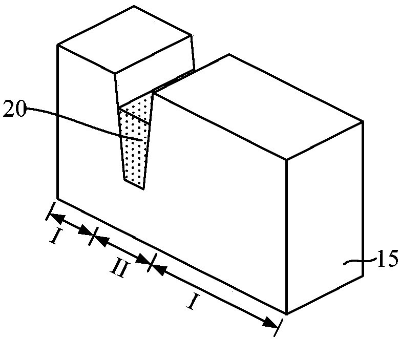
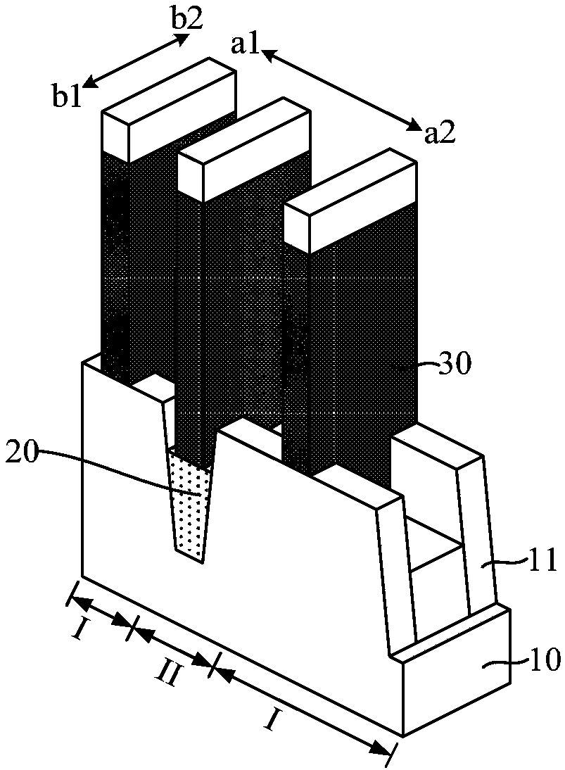
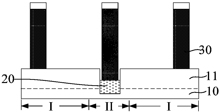
[0018] As the device size decreases, the distance between adjacent transistors also decreases. For FinFETs, the distance between adjacent fins is getting smaller and smaller, and the distance between adjacent gate structures is also getting smaller. Specifically, along the extending direction of the fins, the distance (Head to Head, HTH) between the ends of the adjacent fins becomes smaller and smaller, and the reduction of the distance between the ends of the adjacent fins will make it easy to appear between adjacent devices. Bridging problems, resulting in degradation of electrical performance and yield of semiconductor devices. For this reason, a single-diffusion fracture isolation structure is currently introduced.

[0019] combined referenc...


PUM


Abstract

The invention relates to a semiconductor structure and a forming method thereof. The forming method comprises the steps of: providing a base comprising a substrate and a plurality of discrete fins onthe substrate, wherein the base comprises adjacent device regions and a single diffusion break region; forming a plurality of discrete gate structures across the fins, wherein the gate structures cover part of the top portions and part of the side walls of the fins of the device regions and the single diffusion break region; forming source and drain doped regions in the fins on two sides of the gate structures of the device regions; forming first dielectric layers covering the side walls of the gate structures on the substrate after forming the source and drain doped regions; sequentially etching the gate structure of the single diffusion break region, the fins positioned at the lower portions of the gate structures and the substrate with partial thickness, wherein the first dielectric layers, the fins and the residual substrate of the single diffusion break region form a groove; forming a single diffusion break structure in the groove. By forming the source and drain doped regions firstly, the position accuracy of the groove can be improved, so that the isolation effect of the single diffusion break structure is improved.

Description

technical field [0001] The invention relates to the field of semiconductor manufacturing, in particular to a semiconductor structure and a forming method thereof. Background technique [0002] In semiconductor manufacturing, with the development trend of VLSI, the feature size of integrated circuits continues to decrease. In order to accommodate the reduction in feature size, the channel length of MOSFETs has also been shortened accordingly. However, as the channel length of the device is shortened, the distance between the source and the drain of the device is also shortened, so the control ability of the gate to the channel becomes worse, and the gate voltage pinches off the channel. Difficulty is also increasing, making the phenomenon of subthreshold leakage (subthreshold leakage), the so-called short-channel effects (short-channel effects, SCE) more likely to occur. [0003] Therefore, in order to better adapt to the reduction of the feature size, the semiconductor pro...

Claims


Application Information

Patent Timeline
Patent Type & Authority Applications(China)
IPC IPC(8): H01L29/06H01L29/10H01L29/423H01L29/78H01L21/336H01L21/28
CPCH01L29/785H01L29/0642H01L29/42356H01L29/1033H01L29/66795
Inventor 邓武锋何德飚肖长永
Owner SEMICON MFG INT (SHANGHAI) CORP
Why Eureka
Try Eureka