Fine structure body-producing method, fine structure body, display device, recording device-producing method, and recording device

A microstructure and recording device technology, applied in the direction of the base layer of the recording layer, magnetic recording, magnetic recording layer, etc., can solve the problem of difficulty and no control of the formation position of carbon nanoplates, and achieve the same display characteristics and excellent display quality. , the effect of improving position accuracy

Inactive Publication Date: 2006-10-11
SONY CORP
View PDF0 Cites 5 Cited by
  • Summary
  • Abstract
  • Description
  • Claims
  • Application Information

AI Technical Summary

Problems solved by technology

[0013] However, in Document 7, since the formation position of the carbon nanoplate is not controlled, it is difficult to apply it to the FED.

Method used


Image

  • Fine structure body-producing method, fine structure body, display device, recording device-producing method, and recording device
  • Fine structure body-producing method, fine structure body, display device, recording device-producing method, and recording device
  • Fine structure body-producing method, fine structure body, display device, recording device-producing method, and recording device

Examples


no. 1 example

[0075]

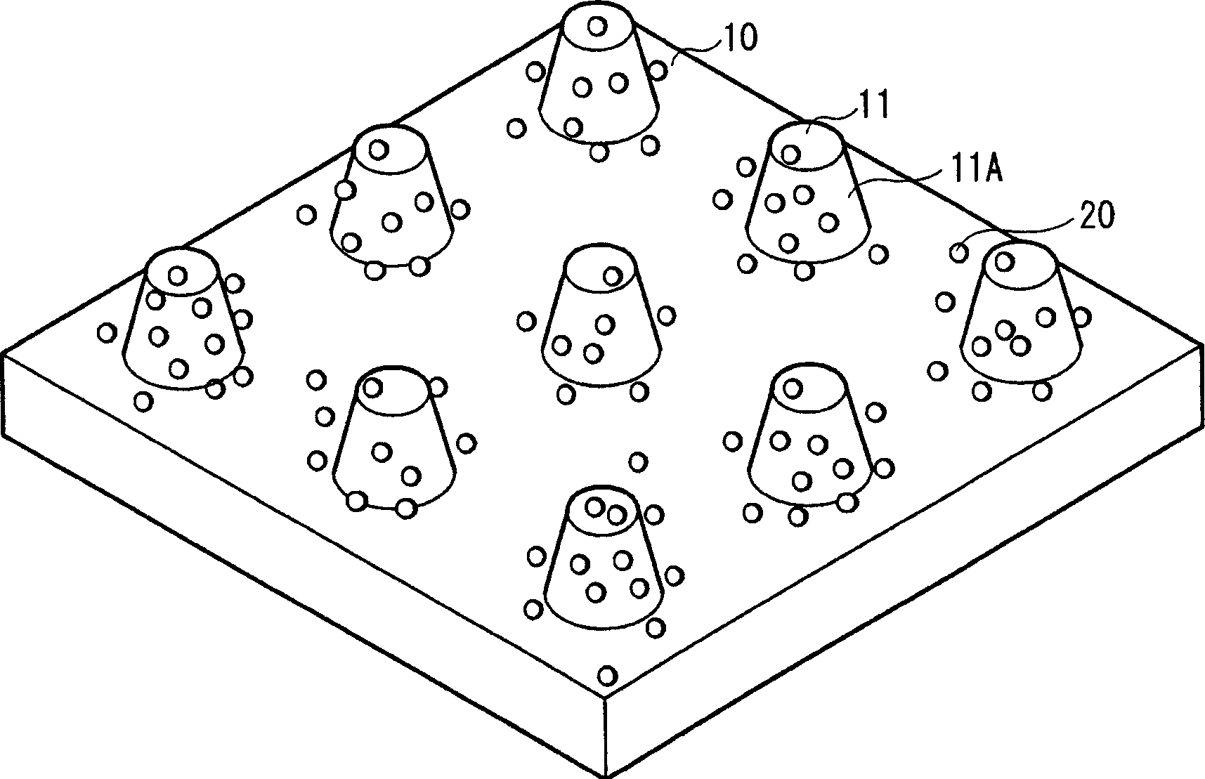
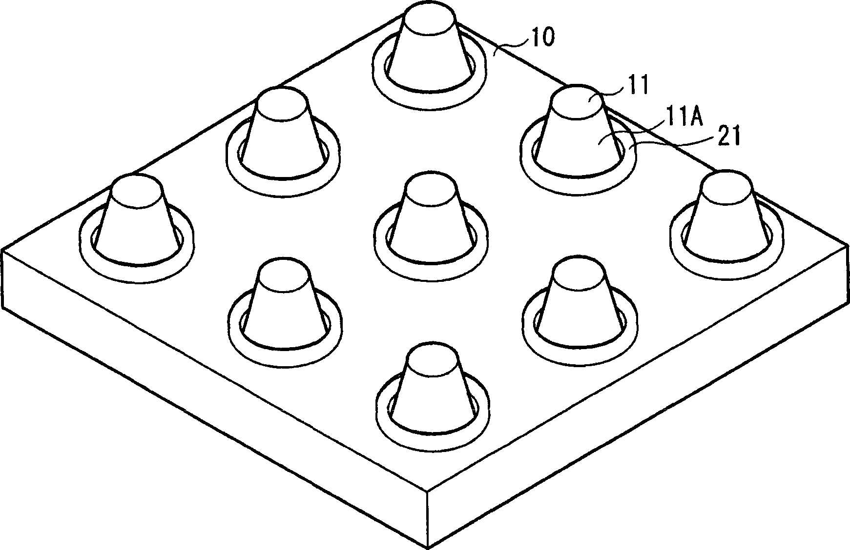
[0076] Figures 1 to 3 A method of manufacturing a fine structure according to a first embodiment of the present invention is shown. The method of this embodiment tends to form a fine structure of, for example, a field electron emission device used as an FED. The method of this embodiment includes a "protrusion forming step" in which a protrusion is formed on a substrate, and a material made of a catalytic effect (hereinafter referred to as "catalyst material") is formed on the side of the protrusion. The "catalyst pattern forming step" of the linear catalyst pattern, and the "tubular structure forming step" of growing a tubular structure using the catalyst pattern.

[0077] (Protrusion forming step)

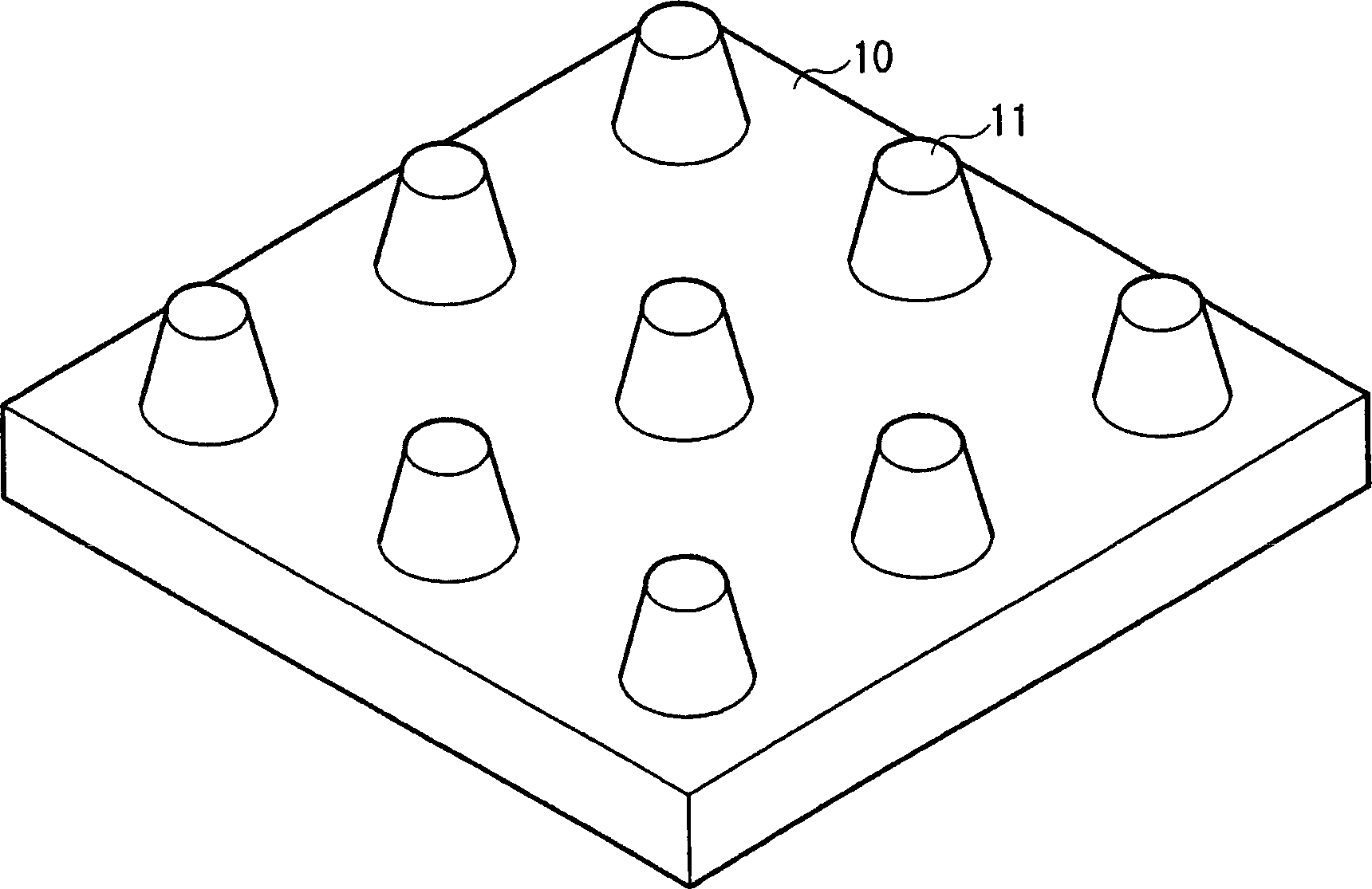
[0078] First, if figure 1 As shown, a substrate 10 made of a semiconductor such as silicon is prepared. On the substrate 10, the bumps 11 are formed in a cyclic array state by, for example, photolithography and etching.

[0079] The shape of the protrusion 11 is ...

no. 2 example

[0106]

[0107] Figure 6 to Figure 10 A method of manufacturing a microstructure according to a second embodiment of the present invention is shown. Except that in the protrusion forming step, the semiconductor layer 110A is formed on the substrate 110 made of an insulating material, and the semiconductor layer 110A is etched until the surface of the substrate 110 is exposed and the protrusion 111 is formed, the method of the present embodiment Same as that of the first embodiment. Therefore, the same symbols denote the same components, and descriptions thereof are omitted.

[0108] (Protrusion forming step)

[0109] First, if Figure 6 As shown, for example, a substrate 110 made of an insulating material is prepared. A semiconductor layer 110A made of, for example, polysilicon is formed on the substrate 110 by, for example, a CVD method, a plasma CVD (PECVD: Plasma Enhanced Chemical Vapor Deposition) method, or a sputtering method. Thereafter, if Figure 7 As shown, ...

no. 3 example

[0120]

[0121] Figures 11 to 14 A method of manufacturing a microstructure according to a third embodiment of the present invention is shown. In addition to forming two steps 211A and 211B in the protrusion 211, forming a catalyst pattern 221A on the side surfaces 211AA and 211BA of the steps 211A and 211B, respectively, and using the catalyst pattern to form a double-layer tubular structure 230, this embodiment is the same as the first embodiment. Example is the same. Therefore, the same symbols denote the same components, and descriptions thereof are omitted.

[0122] (Protrusion forming step)

[0123] First, if Figure 11 As shown, the substrate 10 is subjected to photolithography and etched to form protrusions 211 having first steps 211A and second steps 211B in a periodic array state. The protrusion 211 has a shape in which, for example, a columnar first step 211A and a columnar second step 211B having different diameters from each other are stacked in descending ...


PUM

PropertyMeasurementUnit
thicknessaaaaaaaaaa
diameteraaaaaaaaaa
thicknessaaaaaaaaaa

Abstract

A method of manufacturing a fine structure capable of precisely controlling the position where a tubular structure made of carbon or the like is formed. A cylindrical raised portion (11) is formed on a substrate (10). Subsequently, a catalytic substance (20) such as iron (Fe) is adhered on the substrate (10). Thereafter, the substrate (10) is heat-treated to melt and bond the catalytic substance (20) to the side (11A) of the raised portion (11). This causes a ring-shaped catalyst pattern made of the catalytic substance (20) to be formed on the side (11A) of the raised portion (11). Subsequently, the hollow cylindrical tubular structure (30) is grown using the catalyst pattern. A tubular structure (30) rises from the side (11A) of the raised portion (11) and grows as a carbon (nano)tube having an open head (30A). A tubular structure (30) is formed that corresponds exactly to the position of the raised portion (11).

Description

technical field [0001] The present invention relates to a method of producing a fine structure in which a tubular structure made of carbon or the like is formed by using a catalyst, a fine structure produced by the method, and a method of using the fine structure as a field electron emission The display unit of the device. Furthermore, the present invention relates to a method of manufacturing a recording device using a method of manufacturing a fine structure and a recording device obtained by the method. Background technique [0002] In recent years, nanotechnology has improved significantly. In particular, since molecular structures such as carbon nanotubes are suitable materials having excellent properties such as thermal conductivity, electrical conductivity, and mechanical strength, these structures are expected to be applied to a wide range of applications such as transistors, memories, field electron emission devices. [0003] For example, regarding the use of carb...

Claims


Application Information

Patent Timeline
Patent Type & Authority Applications(China)
IPC IPC(8): B82B3/00B82B1/00B82Y10/00B82Y40/00B82Y99/00G11B5/65G11B5/73G11B5/855H01J1/304H01J9/02H01J29/04H01J31/12
CPCG11B5/855H01J1/3042H01J9/025Y10T428/24744B82B1/00B82B3/00B82Y10/00
Inventor 达拉姆·P·戈塞恩梶浦尚志村上洋介阿多诚文
Owner SONY CORP
Why Eureka
Try Eureka