Double-electron-transport-layer inorganic perovskite solar cell and preparation method thereof, and application of double-electron-transport-layer inorganic perovskite solar cell

A technology of solar cells and double electron transmission, applied in circuits, photovoltaic power generation, electrical components, etc., can solve the problems of low photoelectric conversion efficiency of devices, hindering electron transmission, and large energy levels, so as to improve energy conversion efficiency, reduce recombination, The effect of improving crystallization performance

Active Publication Date: 2019-10-15
SOUTH CHINA UNIV OF TECH
View PDF5 Cites 6 Cited by
  • Summary
  • Abstract
  • Description
  • Claims
  • Application Information

AI Technical Summary

Problems solved by technology

However, under this structure, SnO 2 The conduction band energy level (-4.43eV) does not match the perovskite conduction band energy level (-3.29eV), and there is a large energy level gap, which hinders the transmission of electrons to a certain extent and reduces the photoelectric conversion efficiency of the device.

Method used


Image

  • Double-electron-transport-layer inorganic perovskite solar cell and preparation method thereof, and application of double-electron-transport-layer inorganic perovskite solar cell
  • Double-electron-transport-layer inorganic perovskite solar cell and preparation method thereof, and application of double-electron-transport-layer inorganic perovskite solar cell
  • Double-electron-transport-layer inorganic perovskite solar cell and preparation method thereof, and application of double-electron-transport-layer inorganic perovskite solar cell

Examples


Embodiment 1

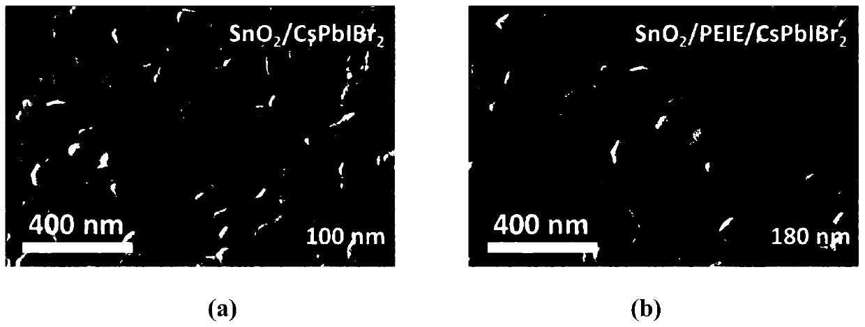
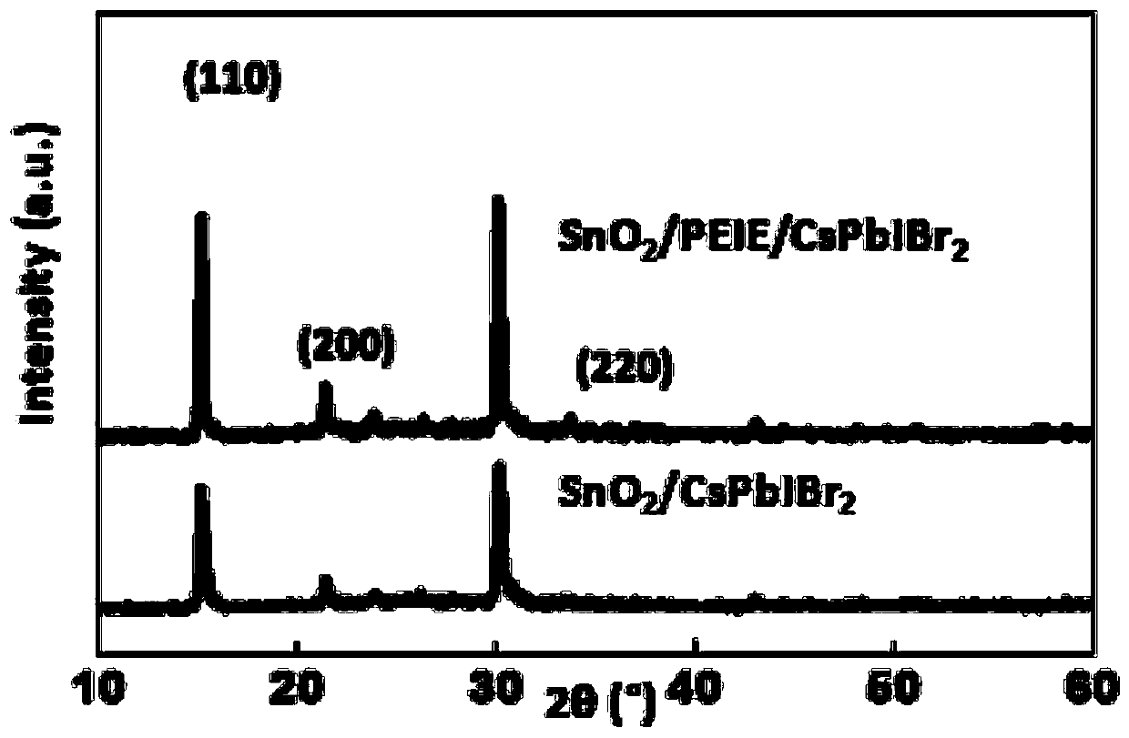
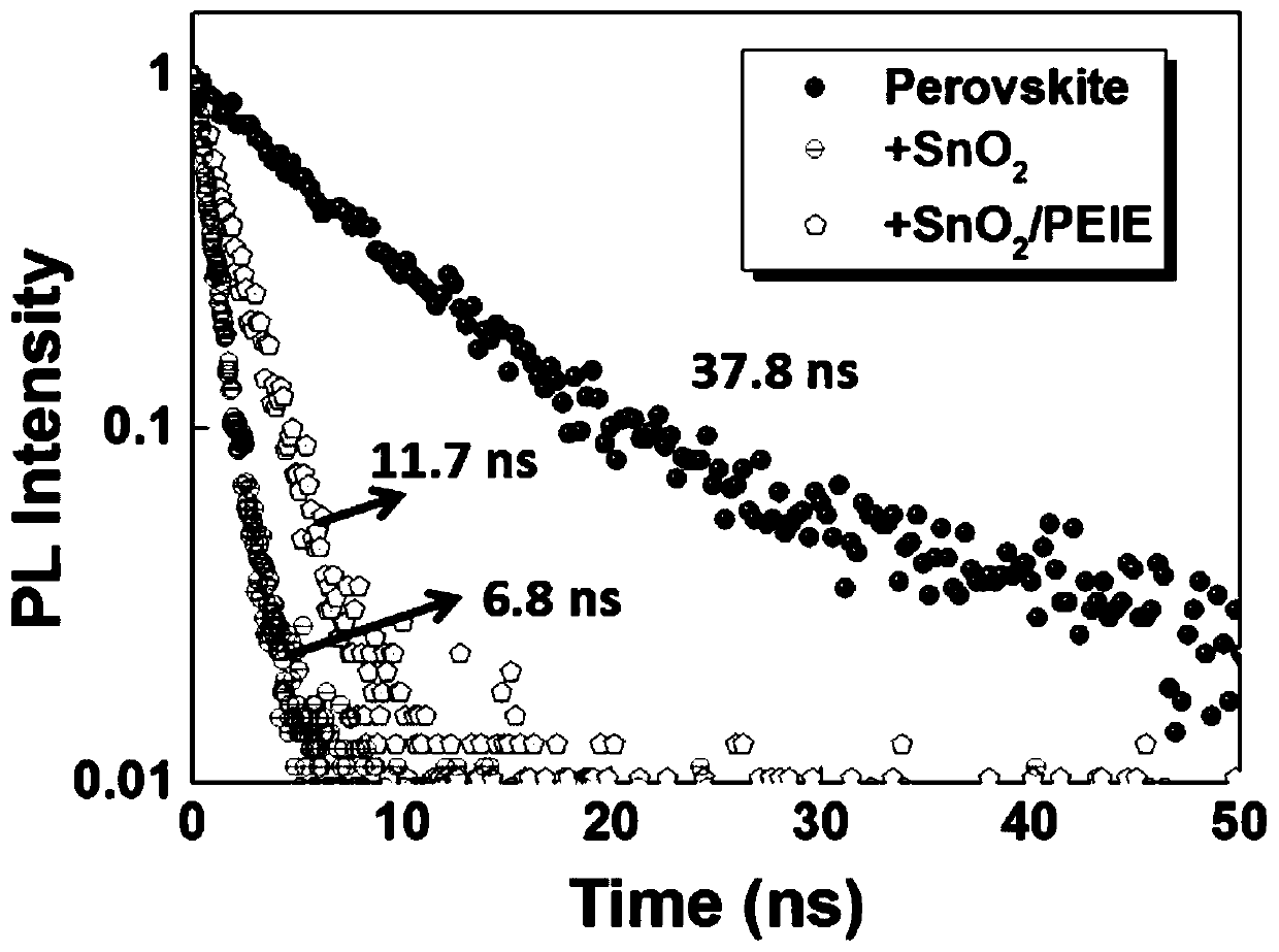
[0062] Implemented device structure: Glass / ITO / SnO 2 / PEIE / CsPbIBr 2 / Spiro-OMeTAD / MoO 3 / Ag

[0063] Preparation steps:

[0064] (1) Clean the glass substrate covered with the ITO film with isopropanol, micron semiconductor professional detergent, deionized water, and isopropanol ultrasonically for 15 to 30 minutes in sequence, and then place it in a constant temperature oven to dry for later use.

[0065] (2) Before use, put the dried ITO flakes in a petri dish and process them in a vacuum plasma cleaner for 3 to 4 minutes. Then the diluted SnO 2 The solution was spin-coated on the surface of ITO, the spin-coating speed was 3000r / min, and the time was 30s to obtain SnO with a thickness of 35nm. 2 Electron transport layer; then 0.5 mg / mL PEIE solution was spin-coated on SnO 2 On the surface of the electron transport layer, the spin coating speed is 3000r / min, the time is 30s, the PEIE thickness is 7nm, and the PEIE electron transport layer is prepared; annealed at 150°C...


PUM

PropertyMeasurementUnit
thicknessaaaaaaaaaa
thicknessaaaaaaaaaa
thicknessaaaaaaaaaa

Abstract

The invention belongs to the technical field of preparation of all-inorganic perovskite solar cell devices, and particularly relates to a double-electron-transport-layer inorganic perovskite solar cell and a preparation method thereof, and application of a double-electron-transport-layer inorganic perovskite solar cell. The double-electron-transport layer (SnO2-PEIE) is obtained by spin coating ofa cathode layer by adopting a solution processing method and annealing in the atmosphere. By adding the PEIE layer, the energy level difference between the SnO2 electron transport layer and the perovskite layer can be reduced, better energy level matching is achieved, the electron extraction capability is enhanced, the electron-hole coincidence in the perovskite light absorption layer is reduced,the photoelectric conversion efficiency of the CsPbIBr2 solar cell is improved, and therefore, the all-inorganic perovskite solar cell device with a high photovoltaic performance is obtained.

Description

technical field [0001] The invention belongs to the technical field of preparation of all-inorganic perovskite solar cell devices, in particular to an inorganic perovskite solar cell with a double electron transport layer and its preparation method and application. Background technique [0002] Stepping into the 21st century, human society and science and technology continue to progress and develop, but what follows is the increasingly serious problem of energy scarcity and environmental pollution. The most effective means to solve this pair of problems is to vigorously develop and promote clean energy and renewable energy. As the most abundant clean energy and renewable energy on earth, solar energy has attracted the attention of scientists from all over the world. In the effective use of solar energy, solar cells can convert solar energy into electrical energy for human use through the photoelectric effect of materials. Therefore, solar cells have become the fastest grow...

Claims


Application Information

Patent Timeline
Patent Type & Authority Applications(China)
IPC IPC(8): H01L51/46H01L51/42H01L51/48
CPCH10K71/12H10K85/141H10K30/30H10K30/35Y02E10/549
Inventor 周颖芝王晶薛启帆
Owner SOUTH CHINA UNIV OF TECH
Why Eureka
Try Eureka