Optoelectronic semiconductor chip

An optoelectronic semiconductor, semiconductor technology, applied in semiconductor devices, semiconductor lasers, circuits, etc., can solve problems such as injuries

Pending Publication Date: 2019-10-15
OSRAM OPTO SEMICON GMBH & CO OHG
View PDF8 Cites 3 Cited by
  • Summary
  • Abstract
  • Description
  • Claims
  • Application Information

AI Technical Summary

Problems solved by technology

[0003] In the case of optoelectronic semiconductor chips emitting infrared radiation with a high power density, there is the risk that body parts, such as in particular the eyes, are exposed to high radiation power and are injured in this case

Method used


Image

  • Optoelectronic semiconductor chip
  • Optoelectronic semiconductor chip
  • Optoelectronic semiconductor chip

Examples


Embodiment Construction

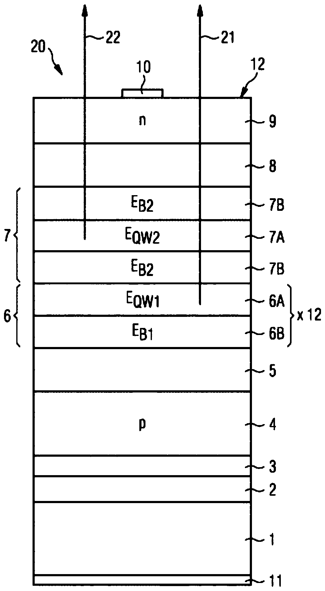
[0030] exist figure 1 The optoelectronic semiconductor chip 20 shown in FIG. 1 according to an exemplary embodiment is a light-emitting diode chip which is designed to emit infrared radiation. In particular, the optoelectronic semiconductor chip 20 is an IR radiation-emitting diode (IRED). The optoelectronic semiconductor chip 20 has a p-type semiconductor region 4 , an n-type semiconductor region 9 and an active layer 6 arranged between the p-type semiconductor region 4 and the n-type semiconductor region 9 which is suitable for emitting IR radiation. An embodiment of the optoelectronic semiconductor chip 20 is a so-called thin-film semiconductor chip, from which the growth substrate originally used for the epitaxial growth of the semiconductor layer has been detached and the semiconductor layer has been bonded instead by means of a connection layer 2 , in particular a solder layer. The sequences are connected to a carrier substrate 1 different from the growth substrate.

...


PUM


Abstract

The invention relates to an optoelectronics semiconductor chip (10), comprising: a p-type semiconductor region (4), an n-type semiconductor region (9), an active layer (6) which is arranged between the p-type semiconductor region (4) and the n-type semiconductor region (9), is formed as a multiple quantum well structure (6A, 6B) and which has alternating quantum well layers (6A) and barrier layers(6B), wherein the quantum well layers (6A) are suitable for the emission of first radiation (21) in a first wavelength range, and at least one further quantum well layer (7A), which is arranged outside the multiple quantum well structure (6A, 6B) and is suitable for the emission of second radiation (22) in a second wavelength range, wherein the first wavelength range lies in the infrared spectralrange, which is invisible to the human eye, and the second wavelength range comprises wavelengths which are at least partly visible to the human eye.

Description

technical field [0001] The invention relates to an optoelectronic semiconductor chip, in particular an optoelectronic semiconductor chip which is suitable for emitting infrared radiation. [0002] This application claims priority from German patent application 10 2017 103 856.6, the disclosure content of which is hereby incorporated by reference. Background technique [0003] In the case of optoelectronic semiconductor chips emitting infrared radiation with a high power density, there is the risk that body parts, such as in particular the eyes, are exposed to high radiation power and are injured in this case. This risk therefore exists in particular in the use of optoelectronic semiconductor chips emitting infrared radiation, since infrared radiation is invisible to the human eye. Contents of the invention [0004] The invention is based on the object of proposing an optoelectronic semiconductor chip emitting infrared radiation, during operation of which the risk of damag...

Claims


Application Information

Patent Timeline
IPC IPC(8): H01L33/06
CPCH01L33/06H01L33/30H01S5/343H01S5/4087H01L33/0008H01L33/08H01L33/0025H01L33/14
Inventor 安德烈亚斯·鲁道夫马库斯·布勒尔沃尔夫冈·施密德约翰内斯·鲍尔马丁·鲁道夫·贝林格
Owner OSRAM OPTO SEMICON GMBH & CO OHG
Why Eureka
Try Eureka