Flexible capacitive type proximity sensor based on capacitor fringe field effect, and sensing method
A proximity sensor and fringe field effect technology, used in electrical/magnetic exploration, instruments, scientific instruments, etc., can solve the problems of large size, less research on flexible proximity sensing, and difficulty in applying wearable devices, and achieve high sensitivity. Effect
- Summary
- Abstract
- Description
- Claims
- Application Information
AI Technical Summary
Problems solved by technology
Method used
Image
Examples
Embodiment 1
[0025] Example 1: Constructing a Capacitive Proximity Sensor Using a Flat Film-like Flexible Stretchable Medium Layer
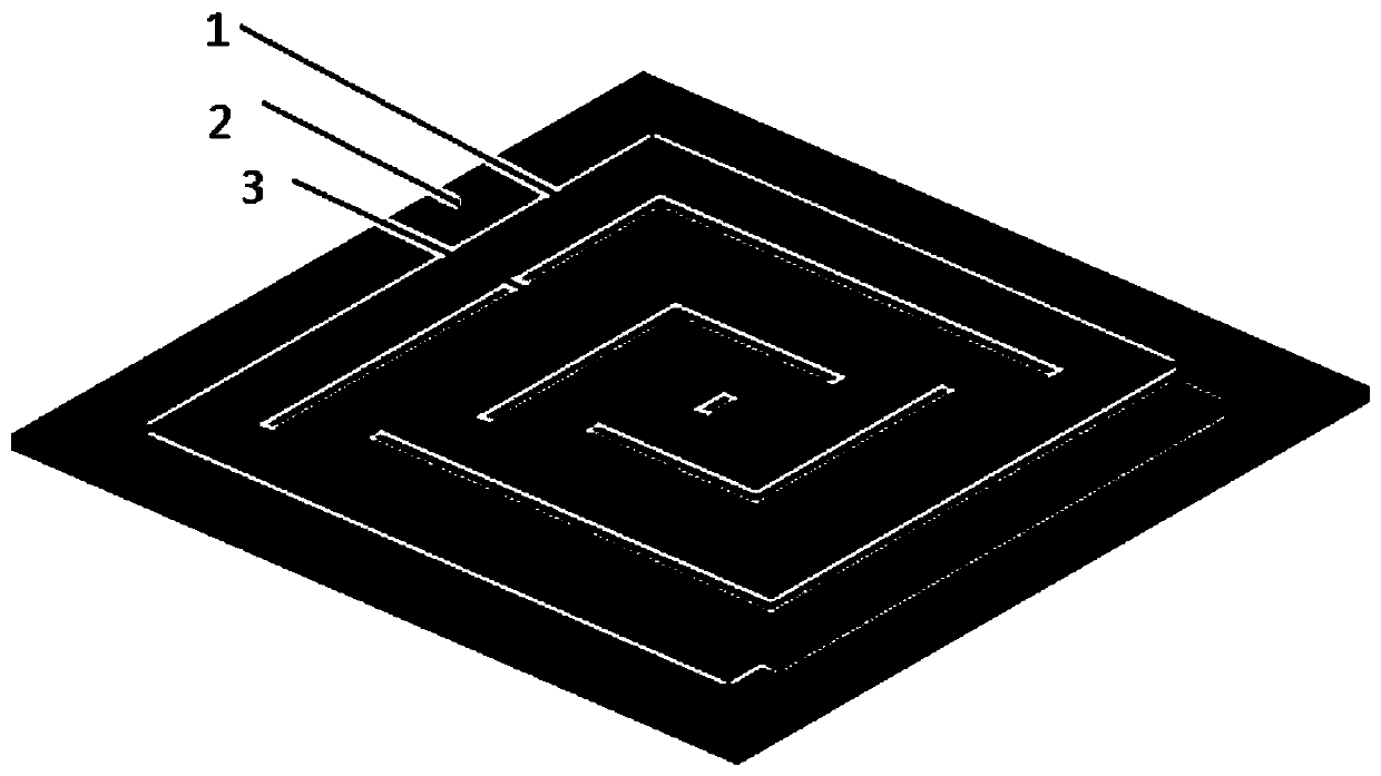
[0026] Taking the patterned electrodes of the square helical shape 1 and 3 on the upper and lower surfaces of the flexible dielectric material as an example, refer to the attached figure 1 The planar film-like flexible and stretchable dielectric layer 2 is designed to construct a capacitive proximity sensor, and the preparation steps are as follows:
[0027] (1) Pour polydimethylsiloxane prepolymer (PDMS, the commonly used model is Sylgard 184, the ratio of crosslinking agent to prepolymer is 1:10) on a plane, vacuumize, remove air bubbles, Place it for 4 hours, then put it in an oven at 50-80°C, and cure it for 2-4 hours;
[0028] (2) Remove the cured PDMS film, cut it to a suitable size, paste a physical mask plate with a spiral pattern on one side of the PDMS film, sputter a spiral metal film electrode with a thickness of 30-80 nanometers, Such as gold, ...
Embodiment 2
[0032] Example 2: Using a flexible and stretchable dielectric layer with a microstructure to construct a capacitive proximity sensor
[0033] Taking the quadrangular pyramid-shaped microstructure distributed on the square helical patterned area on the upper surface of the flexible dielectric material and the square helical patterned metal thin film electrodes on the upper and lower surfaces of the flexible dielectric material as examples, refer to the attached Figure 4 The design uses a flexible and stretchable dielectric layer with a microstructure to construct a capacitive proximity sensor. The preparation steps are:
[0034] (1) Using crystalline silicon oxide wafers, the surface is a thermal oxide layer with a thickness of about 350-450 nanometers, and the silicon oxide wafers are cleaned and dried;
[0035] (2) Spin-coat S1813 photoresist on the surface of the silicon oxide wafer, the spin-coating speed is 3000-5000 rpm, the spin-coating time is 30-60 seconds, and bake ...
PUM
| Property | Measurement | Unit |
|---|---|---|
| Thickness | aaaaa | aaaaa |
Abstract
Description
Claims
Application Information


