A method for increasing the working voltage of dielectric thin film devices under strong electric field

A thin film device, working voltage technology, applied in the direction of fixed capacitor dielectrics, thin film/thick film capacitors, capacitors, etc., can solve the problems of inability to obtain large-area thin films and cannot be used in practical applications, and achieves suppression of thin film leakage current increase, The effect of suppressing leakage current and easy operation

Active Publication Date: 2021-03-19
SICHUAN UNIV +1
View PDF7 Cites 0 Cited by
  • Summary
  • Abstract
  • Description
  • Claims
  • Application Information

AI Technical Summary

Problems solved by technology

However, the limitation of this scheme is that its film preparation method cannot obtain large-area films, and it cannot be used in practical applications at present.

Method used


Image

  • A method for increasing the working voltage of dielectric thin film devices under strong electric field
  • A method for increasing the working voltage of dielectric thin film devices under strong electric field
  • A method for increasing the working voltage of dielectric thin film devices under strong electric field

Examples


Embodiment 1

[0031] The steps of this embodiment are as follows:

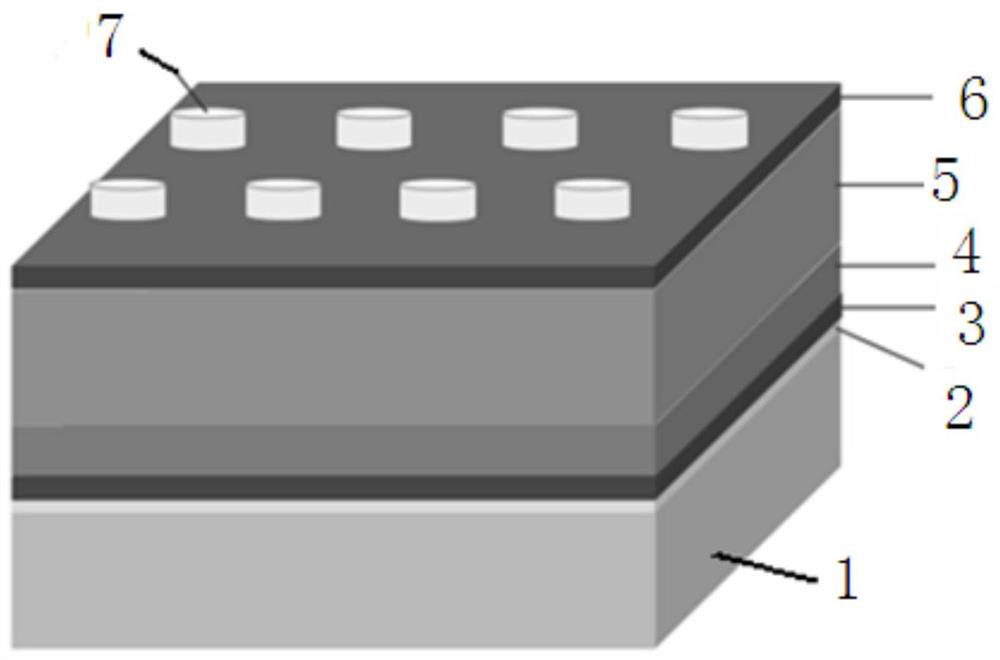
[0032] (1) On the Si substrate prepared with the first metal electrode Pt electrode, the first SrTiO with a thickness of 30 nm was sequentially prepared by radio frequency sputtering method (JGP-560C10 ultra-high vacuum multifunctional magnetron sputtering equipment) 3 layer, LaNiO with a thickness of 60nm 3 Transition layer, PbTiO with a thickness of 550nm 3 thin film, second SrTiO with a thickness of 30 nm 3 layer; preparation of the first SrTiO 3 The process parameters of the layer are: air pressure 2Pa, power 40W, substrate temperature 550°C, sputtering time 15min, Ar:O 2 =40:10 (volume ratio); prepare LaNiO 3 The process parameters of the transition layer are: air pressure 2Pa, power 40W, substrate temperature 550°C, sputtering time 30min, Ar:O 2=40:10 (volume ratio); prepare PbTiO 3 The process parameters of the film are: air pressure 2Pa, power 50W, substrate temperature 550°C, sputtering time 180min, Ar:O 2 =...

Embodiment 2

[0043] The steps of this embodiment are as follows:

[0044] (1) On the Si substrate prepared with the first metal electrode Pt electrode, the first SrTiO with a thickness of 10 nm was sequentially prepared by radio frequency sputtering method (JGP-560C10 ultra-high vacuum multifunctional magnetron sputtering equipment) 3 layer, LaNiO with a thickness of 60nm 3 Transition layer, Pb with a thickness of 800nm 0.52 Zr 0.48 TiO 3 Thin film, second SrTiO with a thickness of 10 nm 3 layer; preparation of the first SrTiO 3 The process parameters of the layer are: air pressure 2Pa, power 40W, substrate temperature 550°C, sputtering time 6min, Ar:O 2 =40:10 (volume ratio); prepare LaNiO 3 The process parameters of the transition layer are: air pressure 2Pa, power 40W, substrate temperature 550°C, sputtering time 30min, Ar:O 2 =40:10 (volume ratio); prepare Pb 0.52 Zr 0.48 TiO 3 The process parameters of the film are: air pressure 2Pa, power 50W, substrate temperature 500°C, s...

Embodiment 3

[0055] The steps of this embodiment are as follows:

[0056] (1) On the Si substrate prepared with the first metal electrode Pt electrode, the first CaZrO with a thickness of 10 nm was sequentially prepared by radio frequency sputtering (JGP-560C10 ultra-high vacuum multifunctional magnetron sputtering equipment) 3 layer, LaNiO with a thickness of 30nm 3 Transition layer, BaTiO with a thickness of 800nm 3 Thin film, second CaZrO with a thickness of 10 nm 3 layer; preparation of the first CaZrO 3 The process parameters of the layer are: air pressure 2Pa, power 70W, substrate temperature 550°C, sputtering time 10min, Ar:O 2 =40:10 (volume ratio); prepare LaNiO 3 The process parameters of the transition layer are: air pressure 2Pa, power 50W, substrate temperature 550°C, sputtering time 10min, Ar:O 2 =40:10 (volume ratio); prepare BaTiO 3 The process parameters of the film are: air pressure 2Pa, power 50W, substrate temperature 500°C, sputtering time 300min, Ar:O 2 =40:10 ...


PUM

PropertyMeasurementUnit
thicknessaaaaaaaaaa
electric potential / voltageaaaaaaaaaa

Abstract

The invention provides a method for improving the operating voltage of a dielectric thin film device under a strong electric field. A nano-sized oxide insulation layer is prepared between a dielectricthin film and a metal electrode by a radio frequency magnetron sputtering method to form a metal electrode-oxide insulation layer-dielectric thin film-oxide insulation layer-metal electrode structuredielectric thin film device or form a metal electrode-oxide insulation layer-LaNiO3 transition layer-dielectric thin film-oxide insulation layer-metal electrode structure dielectric thin film device.The oxide of preparing the oxide insulation layer is one of SrTiO3, CaZrO3 and SrZrO3. With application of the method, the oxide insulation layer of nanometer thickness is introduced into the dielectric thin film device, thereby effectively suppressing the increase of the thin film leakage current caused by the charge injection from the metal electrode to the dielectric thin film under the actionof the strong electric field, and improve the operating voltage of the dielectric thin film device under the strong electric field.

Description

technical field [0001] The invention belongs to the field of microelectronic devices, and in particular relates to a method for suppressing the leakage current of a dielectric thin film so as to increase the working voltage of a dielectric thin film device. Background technique [0002] Thin-film solid-state dielectric electronic devices, such as film capacitors, film sensors, and film memories, are a new generation of electronic devices with the characteristics of miniaturization, low power consumption, multi-function, and integration. Compared with bulk dielectric devices (such as electronic devices made of ceramic materials, the thickness of which is at least greater than 10 μm), the thickness of thin-film dielectric devices is greatly reduced, usually between several hundred nm and 2 μm, so under the same operating voltage, Thin-film dielectric devices are subject to much larger operating electric fields than bulk dielectric devices (~10 4 -10 5 V / mm). In order to mee...

Claims


Application Information

Patent Timeline
Patent Type & Authority Patents(China)
IPC IPC(8): H01G4/33H01G4/12C23C14/08C23C14/35C23C14/58
CPCC23C14/08C23C14/088C23C14/35C23C14/5806H01G4/1218H01G4/1236H01G4/1245H01G4/33
Inventor 余萍陈潇洋张仪丁明建庄彤莫桃兰
Owner SICHUAN UNIV
Why Eureka
Try Eureka