Semiconductor device and method of forming the same

A semiconductor and device technology, applied in the field of semiconductor devices and their formation, can solve problems such as poor interconnection structure performance, achieve the effects of improving performance, avoiding position shift, and meeting the needs of process design

Active Publication Date: 2021-07-13
SEMICON MFG INT (SHANGHAI) CORP +1
View PDF3 Cites 0 Cited by
  • Summary
  • Abstract
  • Description
  • Claims
  • Application Information

AI Technical Summary

Problems solved by technology

[0004] However, existing interconnect structures perform poorly

Method used


Image

  • Semiconductor device and method of forming the same
  • Semiconductor device and method of forming the same
  • Semiconductor device and method of forming the same

Examples


Embodiment Construction

[0027] As mentioned in the background, semiconductor devices formed in the prior art have poor performance.

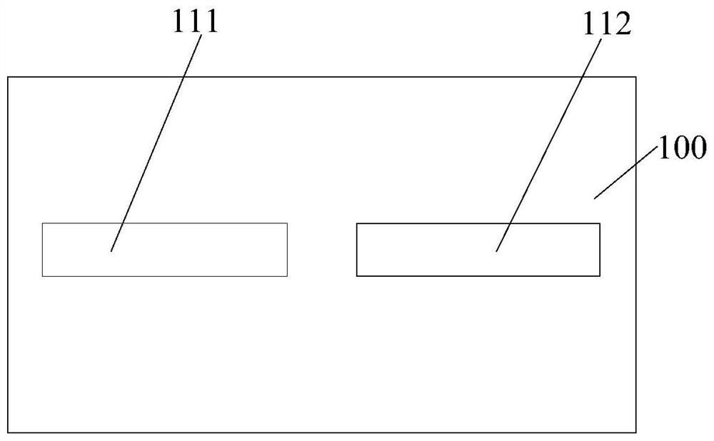
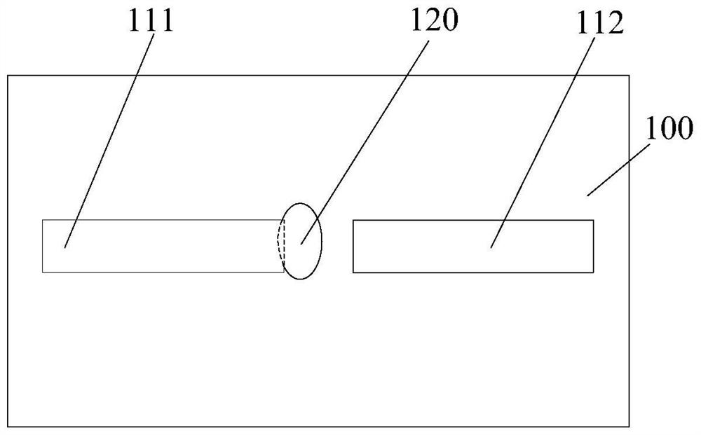
[0028] Figure 1 to Figure 2 It is a structural schematic diagram of the formation process of a semiconductor device.

[0029] refer to figure 1 , providing the layer 100 to be etched.

[0030] continue to refer figure 1 , etch part of the layer to be etched 100, and form discrete first grooves 111 and second grooves 112 in the layer to be etched 100, the extension direction of the first grooves 111 and the second grooves 112 is parallel to the first The arrangement direction between the groove 111 and the second groove 112 .

[0031] refer to figure 2 , forming a via hole 120 in the layer to be etched 100 between the first trench 111 and the second trench 112 .

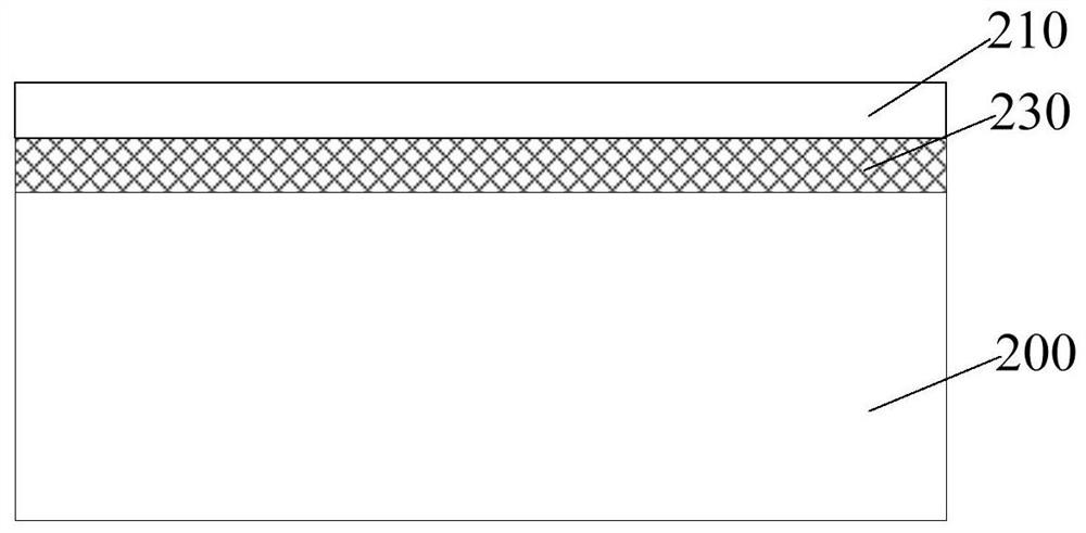
[0032] Subsequent steps also include: forming a first conductive layer in the first trench 111 ; forming a second conductive layer in the second trench 112 ; and forming a conductive plug in the throu...


PUM

PropertyMeasurementUnit
thicknessaaaaaaaaaa
thicknessaaaaaaaaaa

Abstract

A semiconductor device and a forming method thereof, the method comprising: forming a first mask material layer on a layer to be etched, the first mask material layer including a blocking region; forming a discrete first mask in the first mask material layer The film groove and the second mask groove, the extension directions of the first mask groove and the second mask groove are all parallel to the arrangement direction between the first mask groove and the second mask groove, and the first mask groove and the second mask groove A mask groove and a second mask groove are respectively located on both sides of the barrier region; the sidewall is exposed in the barrier region to form a barrier layer; a part of the barrier layer of the first mask material layer is etched using the barrier layer as a mask area, forming a first mask through hole in the barrier area of ​​the first mask material layer; then use the barrier layer and the first mask material layer as a mask to etch the layer to be etched, and in the first mask groove, the second The first groove, the second groove and the through hole are correspondingly formed in the layer to be etched at the bottom of the groove of the second mask and the through hole of the first mask. The method results in improved performance of semiconductor devices.

Description

technical field [0001] The invention relates to the field of semiconductor manufacturing, in particular to a semiconductor device and a forming method thereof. Background technique [0002] Interconnection structures are often required to be formed in semiconductor integrated circuit processes. The interconnect structure is used to electrically connect the upper and lower material layers. The interconnection structure includes a conductive layer and a conductive plug, the conductive layer is located in the trench, and the conductive plug is located in the through hole. [0003] The positions of the through holes and grooves are usually designed according to the needs of the design. Some vias need to be located between adjacent trenches, and the vias and trenches are separated from each other. [0004] However, the performance of existing interconnect structures is poor. Contents of the invention [0005] The problem to be solved by the invention is to provide a semicon...

Claims


Application Information

Patent Timeline
Patent Type & Authority Patents(China)
IPC IPC(8): H01L21/768H01L23/528
CPCH01L21/76816H01L23/5283H01L2221/101H01L21/76897H01L21/486H01L21/76843H01L21/7688
Inventor 张城龙
Owner SEMICON MFG INT (SHANGHAI) CORP
Why Eureka
Try Eureka