Wafer thinning method and wafer structure

A wafer and wafer testing technology, which is applied to machine tools suitable for grinding workpiece planes, semiconductor/solid-state device testing/measurement, manufacturing tools, etc., can solve wafer undercutting, reduce effective chip area, and wafer price Advanced problems, to achieve the effect of reducing the number of edge trimming, increasing the effective chip area, and avoiding lateral undercutting

Active Publication Date: 2022-03-01
WUHAN XINXIN SEMICON MFG CO LTD
View PDF15 Cites 0 Cited by
  • Summary
  • Abstract
  • Description
  • Claims
  • Application Information

AI Technical Summary

Problems solved by technology

[0003] In the implementation of wafer-level packaging technology, after wafer bonding, thinning is carried out from the back of the wafer. In order to obtain a flat surface after thinning, an EPI (Epitaxy, epitaxial) wafer is usually used, that is, on silicon A wafer with an epitaxial layer grown on the substrate. During the thinning process, the epitaxial layer is used as a stop layer for acid etching, so that a flat silicon surface can be obtained. During the etching process of the wafer, it will cause undercutting in the lateral direction of the wafer, which needs to be trimmed by cutting the edge, which will reduce the effective chip area

Method used


Image

  • Wafer thinning method and wafer structure
  • Wafer thinning method and wafer structure
  • Wafer thinning method and wafer structure

Examples


Embodiment Construction

[0041] In order to make the above objects, features, and advantages of the present invention, the specific embodiments of the present invention will be described in detail below with reference to the accompanying drawings.

[0042] Many specific details are set forth in the following description to fully understand the present invention, but the present invention can also be implemented in other than other means described herein, and those skilled in the art can do without violating the connotation of the present invention. Similarly, the present invention is not limited by the specific embodiments disclosed below.

[0043] Next, the present invention is described in connection with the schematic diagram. The scope of the invention is protected. In addition, the three-dimensional spatial dimensions of length, width, and depth should be included in the actual production.

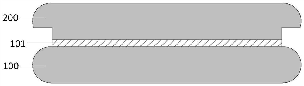
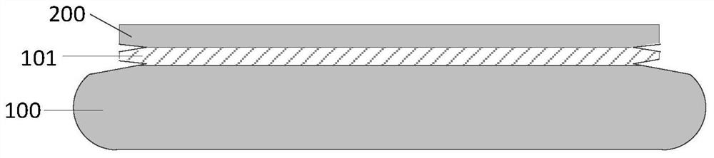
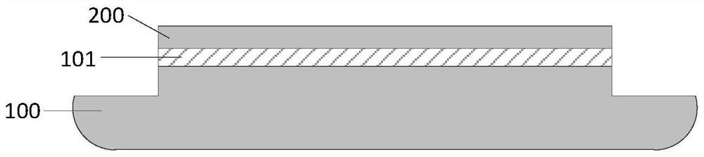
[0044] As described in the background, after the wafer bond, it can be thinned from the back surface of the wa...


PUM

PropertyMeasurementUnit
thicknessaaaaaaaaaa

Abstract

The present invention provides a wafer thinning method and a wafer structure. The embodiment of the present application provides a wafer thinning method. After providing the wafer to be thinned, it can be ground from the back of the wafer, and then the The first planarization process is performed on the back of the wafer to repair the flatness of the wafer after grinding, and then the second planarization process is performed from the back of the wafer until the target thinning thickness is reached. That is to say, the embodiment of the present application can repair the flatness of the wafer through two planarization processes after removing part of the thickness of the wafer, without using an epitaxial layer as an etching stop layer, which reduces the cost of thinning, while Grinding removes most of the thickness without using acid etching, avoiding the lateral undercutting caused by acid etching, thereby reducing the number of edge trimmings caused by lateral undercutting and increasing the effective chip area.

Description

Technical field [0001] The present invention relates to a semiconductor device and a manufacturing range thereof, and more particularly to a thin wafer thinning method and a wafer structure. Background technique [0002] With the continuous development of semiconductor technology, 3D-IC (3D integrated circuit) technology has been widely used, which use wafer level packaging technology to combine different wafers, which has high performance, low cost. And the advantage of high integration. [0003] In the implementation of the wafer stage package technology, after the wafer bond, thinned from the back surface of the wafer, in order to obtain a flat surface after thinning, EPI (Epitaxy, epitaxial) wafer is usually used, ie in silicon The wafer of the epitaxial layer is grown on the substrate, and during thinning, the epitaxial layer is etched as an acid method, so that the flat silicon surface can be obtained, however, the wafer of the EPI is high, and In the process of etching, th...

Claims


Application Information

Patent Timeline
Patent Type & Authority Patents(China)
IPC IPC(8): H01L21/304H01L21/306H01L21/67
CPCH01L21/304H01L21/30625H01L21/67253B24B7/228H01L21/02002H01L22/12H01L21/76254H01L21/02013H01L21/02016H01L21/68742H01L22/26
Inventor 易洪昇
Owner WUHAN XINXIN SEMICON MFG CO LTD
Why Eureka
Try Eureka