Preparation method of photoresist pattern

A photoresist and photoresist layer technology, applied in the field of photolithography, can solve the problems of inability to obtain a periodic pattern structure, limit the general application of laser interference exposure technology, etc., and achieve a simple and practical preparation method, flat sidewalls, and low cost. Effect

Inactive Publication Date: 2019-10-25
INST OF PHYSICS - CHINESE ACAD OF SCI
View PDF5 Cites 0 Cited by
  • Summary
  • Abstract
  • Description
  • Claims
  • Application Information

AI Technical Summary

Problems solved by technology

from figure 2 It can be seen that the sidewall of the photoresist pattern has a periodic wavy structure, and a good periodic pattern structure cannot be obtained, which greatly limits the general application of laser interference exposure technology.

Method used


Image

  • Preparation method of photoresist pattern
  • Preparation method of photoresist pattern
  • Preparation method of photoresist pattern

Examples


Embodiment 1

[0037] The silicon wafer substrate was cleaned with acetone, alcohol, and deionized water in sequence. AR-3840 photoresist was spin-coated on the silicon wafer substrate at a spinning speed of 4000r / min, and the photoresist was baked and cured to obtain a first photoresist layer with a thickness of 500 nm.

[0038] A gold intercalation layer with a thickness of 30 nm was deposited by electron beam evaporation on the first photoresist layer.

[0039] A diluted photoresist (AR-3840: deionized water volume ratio of 1:5) was spin-coated on the gold intercalation layer to obtain a second photoresist layer with a thickness of about 100 nm.

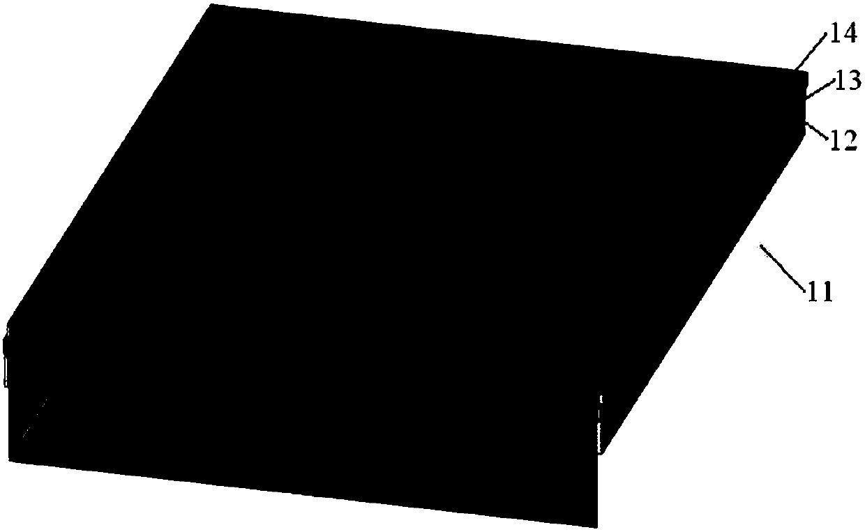
[0040] image 3 is a schematic diagram of the structure of a multilayer photoresist layer. like image 3 As shown, it includes a silicon substrate 11 , a first photoresist layer 12 , a gold intercalation layer 13 and a second photoresist layer 14 from bottom to top.

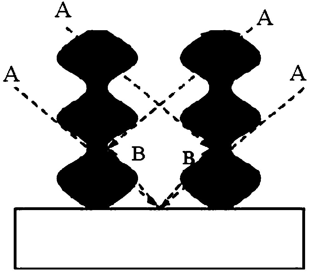
[0041] The second photoresist layer 14 is exposed once by using a double-b...

Embodiment 2

[0048] It is basically the same as Embodiment 1, except that the thickness of the first photoresist layer is 200 nanometers.

Embodiment 3

[0050] It is basically the same as Embodiment 1, except that the thickness of the first photoresist layer is 2 microns.


PUM

PropertyMeasurementUnit
thicknessaaaaaaaaaa
thicknessaaaaaaaaaa
thicknessaaaaaaaaaa

Abstract

The invention provides a preparation method of a photoresist pattern. The preparation method comprises the following steps: 1) forming a first photoresist layer on a substrate; 2) depositing a mask layer on the first photoresist layer; 3) forming a second photoresist layer on the mask layer; 4) forming a second photoresist pattern on the second photoresist layer by using the double-beam laser interference exposure; 5) transferring the second photoresist pattern to the mask layer to form a mask pattern; 6) forming a first photoresist pattern on the first photoresist layer by taking the mask pattern as a mask. According to the preparation method disclosed by the invention, a large-area nano-scale pattern structure can be efficiently obtained, and the influence of the inherent standing wave effect of a laser interference exposure device on the side wall of the micro-nano-scale photoresist pattern is overcome.

Description

technical field [0001] The invention relates to the field of photolithography, in particular to a method for preparing a photoresist pattern. Background technique [0002] At present, photolithography is mainly used to prepare periodic pattern structures on planar substrates. Commonly used lithography techniques include contact UV lithography, stepping UV lithography, electron beam exposure, focused ion beam exposure, and laser interference lithography. The cost of contact UV lithography is low and the efficiency is high, but the resolution can only reach the order of 1 micron; the resolution of step UV lithography, electron beam exposure and focused ion beam exposure can reach several to tens of nanometers , but its equipment is very expensive, and for step-by-step scanning exposure, the efficiency is low. Laser interference lithography uses the principle of multi-beam laser interference, and adopts single or multiple exposure technology between coherent beams, which can ...

Claims


Application Information

Patent Timeline
Patent Type & Authority Applications(China)
IPC IPC(8): G03F7/20
CPCG03F7/2022G03F7/70408
Inventor 乐艮贾海强陈弘
Owner INST OF PHYSICS - CHINESE ACAD OF SCI
Why Eureka
Try Eureka