A Hybrid SRAM Cell Circuit of 10t TFET and MOSFET Devices with High Write Margin

A unit circuit and write margin technology, which is applied in the fields of instruments, static memory, digital memory information, etc., can solve the problems of increased chip cost, weak unit write capability, and increased transmission tube size, achieving a huge area and good performance. Effect

Active Publication Date: 2021-04-30
ANHUI UNIVERSITY
View PDF3 Cites 0 Cited by
  • Summary
  • Abstract
  • Description
  • Claims
  • Application Information

AI Technical Summary

Problems solved by technology

Although this structure perfectly solves the problem of the P-I-N forward bias current of TFETs, stacking TFETs leads to very weak writing ability of the cells, and the cells cannot even be written successfully in the smallest size (as shown in Table 1)
In order to realize the write function, the size of the transmission tube must be increased, resulting in an increase in unit area and an increase in chip cost

Method used


Image

  • A Hybrid SRAM Cell Circuit of 10t TFET and MOSFET Devices with High Write Margin
  • A Hybrid SRAM Cell Circuit of 10t TFET and MOSFET Devices with High Write Margin
  • A Hybrid SRAM Cell Circuit of 10t TFET and MOSFET Devices with High Write Margin

Examples


Embodiment Construction

[0021] The technical solutions in the embodiments of the present invention will be clearly and completely described below in conjunction with the accompanying drawings in the embodiments of the present invention. Obviously, the described embodiments are only some of the embodiments of the present invention, not all of them. Based on the embodiments of the present invention, all other embodiments obtained by persons of ordinary skill in the art without making creative efforts belong to the protection scope of the present invention.

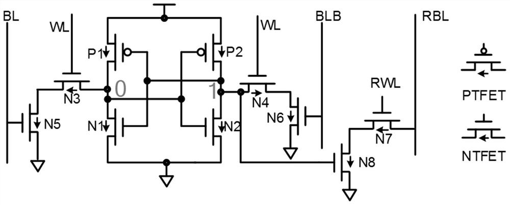
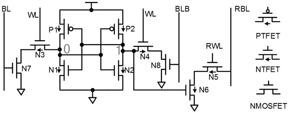
[0022] The used basic device of traditional SRAM memory cell circuit is MOSFET, and the basic device used in the 10T TFET and MOSFET device hybrid SRAM cell circuit that the present invention proposes is a tunneling field effect transistor (TFET). Due to the shortcomings of P-I-N forward bias current and weak conduction capability of stacked TFETs, a method of combining TFETs and MOSFETs for transmission tubes of SRAM units in the embodiment of the ...


PUM


Abstract

The invention discloses a 10T TFET and MOSFET device hybrid SRAM unit circuit with high write margin. The combination of MOSFET devices not only overcomes the shortcoming of weak transmission capability of stacked TFETs, but also avoids the problem of P-I-N forward bias current when TFET devices are used as SRAM unit transmission tubes. The write ability of the unit is improved, and the static power consumption of the unit is reduced.

Description

technical field [0001] The invention relates to the field of integrated circuit design, in particular to a 10T TFET and MOSFET device hybrid SRAM unit circuit with high writing margin. Background technique [0002] With the development of mobile electronic products, people's demand for low power consumption of integrated circuits has become more and more urgent. In recent years, MOSFET (Metal-Oxide Semiconductor Field Effect Crystal) has become an important part of digital integrated circuits and analog integrated circuits. However, with the development of integrated circuit technology nodes, the size of MOSFET is gradually reduced. Due to the short channel effect of MOSFET, its ability to turn off at sub-threshold voltage is weakened, which increases the static leakage current and static power consumption of the circuit. In a microprocessor, static random access memory (SRAM) occupies more than 50% of the chip area and consumes most of the static power consumption of the p...

Claims


Application Information

Patent Timeline
Patent Type & Authority Patents(China)
IPC IPC(8): G11C11/412G11C11/417
CPCG11C11/412G11C11/417
Inventor 卢文娟欧阳春董兰志彭春雨吴秀龙蔺智挺陈军宁
Owner ANHUI UNIVERSITY
Why Eureka
Try Eureka