

Deep trench isolation technical method
A process method, deep groove technology, applied in electrical components, semiconductor/solid-state device manufacturing, circuits, etc., to reduce challenges, reduce difficulty, and save masks
- Summary
- Abstract
- Description
- Claims
- Application Information
AI Technical Summary
Problems solved by technology
Method used
Image

Examples
Embodiment Construction
[0032] The deep trench isolation process method described in the present invention is described as follows in conjunction with the accompanying drawings, and each step corresponds to Figure 1 to Figure 10 , including the following process steps:
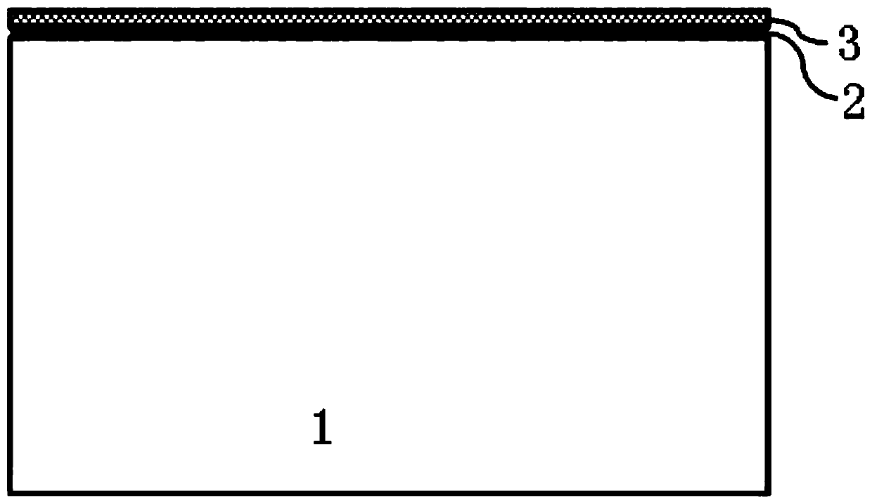
[0033] In step 1, a semiconductor substrate is provided, and a silicon oxide layer and a silicon nitride layer are sequentially formed on the surface of the semiconductor substrate, such as figure 1 shown. Forming the silicon oxide layer and the silicon nitride layer adopts a traditional deposition process to form a film layer with uniform thickness and good quality on the surface of the semiconductor substrate.
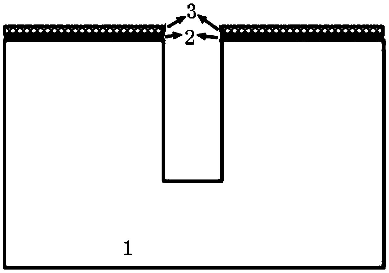
[0034] Step 2: Etch the silicon nitride layer and the silicon oxide layer through the definition of photoresist, open the area where the deep trench is to be formed, etch downward to form a trench with a certain depth, and the depth of the downward etching can be freely It is determined that the downward etching depth i...
PUM
 Abstract
Description
Claims
Application Information