Method for removing photoresist residues and semiconductor device manufacturing method

A technology of photoresist and photoresist layer, which is applied in semiconductor/solid-state device manufacturing, semiconductor devices, electric solid-state devices, etc., can solve problems such as product failure, shedding, and contamination of the wafer film layer structure, and achieve yield improvement Effect

Active Publication Date: 2019-10-29
WUHAN XINXIN SEMICON MFG CO LTD
View PDF10 Cites 6 Cited by
  • Summary
  • Abstract
  • Description
  • Claims
  • Application Information

AI Technical Summary

Problems solved by technology

Moreover, when the photoresist at the edge of the step top W1 of the step is washed and removed by using the edge photoresist removal technology, part of the photoresist will be washed and accumulated at the corner (trimming corner) of the step, and the accumulated photoresist The thickness is also much more than 10μm, such as Figure 1c As shown, the position D3 is the photoresist accumulated at the corner of the bottom W2 of the step. This part of the photoresist will fall off after high-temperature baking in the subsequent process, and become particulate foreign matter to contaminate the film layer on the wafer. structure, resulting in poor product

Method used


Image

  • Method for removing photoresist residues and semiconductor device manufacturing method
  • Method for removing photoresist residues and semiconductor device manufacturing method
  • Method for removing photoresist residues and semiconductor device manufacturing method

Examples


Embodiment Construction

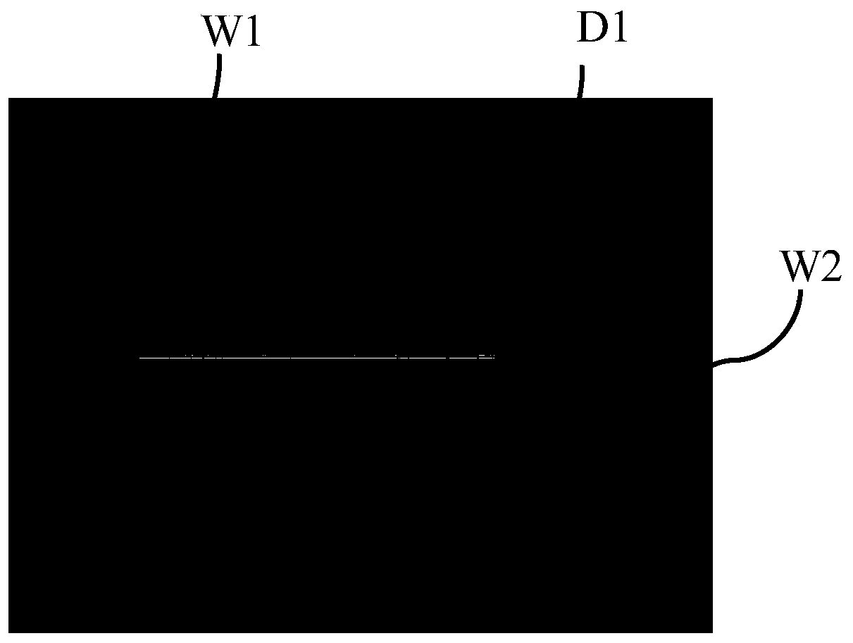
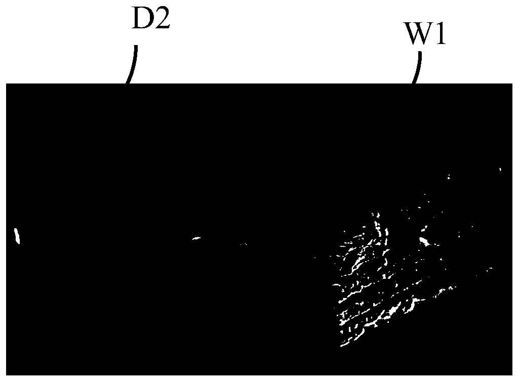
[0032] In order to make the purpose, advantages and characteristics of the present invention clearer, the following in conjunction with the attached Figure 2-4d The method for removing photoresist residue and the method for manufacturing a semiconductor device proposed by the present invention are further described in detail. It should be noted that all the drawings are in a very simplified form and use imprecise scales, and are only used to facilitate and clearly assist the purpose of illustrating the embodiments of the present invention.

[0033] An embodiment of the present invention provides a method for removing photoresist residues, which is used to remove photoresist residues on the edge of a wafer under a certain photolithography process. Refer to figure 2 , figure 2 It is a flowchart of a method for removing photoresist residues according to an embodiment of the present invention, and the steps of the method for removing photoresist residues include:

[0034] Ste...


PUM


Abstract

The invention provides a method for removing photoresist residues and a semiconductor device manufacturing method. The method for removing photoresist residues comprises the steps that a wafer which comprises an intermediate region and an edge region surrounding the intermediate region is provided; a photoresist layer is formed on the intermediate region and the edge region of the wafer; at leasta hydrophilic organic solvent is coated on the photoresist layer in the edge region; and a de-edge process is used to remove the photoresist layer and the organic solvent in the edge region. Accordingto the technical scheme of the invention, the photoresist layer in the edge region of the wafer is completely removed, thereby preventing photoresist residues from affecting a subsequent process.

Description

technical field [0001] The invention relates to the field of integrated circuit manufacturing, in particular to a method for removing photoresist residues and a manufacturing method for semiconductor devices. Background technique [0002] During the processing and manufacturing of semiconductor chips, it is usually necessary to trim (trimming) the edge of the wafer, so as to eliminate the influence of defects on the edge of the wafer on the subsequent bonding (bonding) process. For example, in the manufacturing process of a backside illuminated CMOS image sensor (BSI CIS for short), it is usually necessary to trim the edge of the wafer to remove part of the thickness before the bonding process, so as to avoid causing Defects such as peeling of the wafer edge. [0003] After the wafer edge trimming process, when the photolithography process needs to be carried out in the process of continuing to form a film structure (such as a metal interconnection structure, etc.) on the w...

Claims


Application Information

Patent Timeline
Patent Type & Authority Applications(China)
IPC IPC(8): H01L21/027H01L21/308H01L27/146
CPCH01L21/0273H01L21/0274H01L21/3081H01L21/3086H01L27/14685H01L27/14687
Inventor 熊易斯
Owner WUHAN XINXIN SEMICON MFG CO LTD
Why Eureka
Try Eureka