Method for improving residual microparticles on surface of wafer

A technology of micro-particles and wafers, applied in the manufacture of discharge tubes, electrical components, semiconductor/solid-state devices, etc., can solve the problems of loss of production capacity, rising operating costs, damage to cavity components, etc., and improve the residue of micro-particles on the wafer surface. , The effect of solving particle attachments

Pending Publication Date: 2019-11-01
SHANGHAI HUALI MICROELECTRONICS CORP
View PDF9 Cites 3 Cited by
  • Summary
  • Abstract
  • Description
  • Claims
  • Application Information

AI Technical Summary

Problems solved by technology

[0004] In the process of mass production, the first layer of metal trench etching operation cavity increases with the number of operating hours and wafers, and more and more polymers accumulate on the surface of the cavity, usually through self-cleaning The process performs self-cleaning between wafer batches and between wafers, but too much self-cleaning process will seriously damage the chamber components, especially the electrostatic chuck, which will bring greater density source of defects, and second, it will lead to serious loss of production capacity and rising operating costs

Method used


Image

  • Method for improving residual microparticles on surface of wafer
  • Method for improving residual microparticles on surface of wafer
  • Method for improving residual microparticles on surface of wafer

Examples


Embodiment 1

[0035] The present invention provides a method for improving the residual microparticles on the wafer surface, referring to Figure 7 , Figure 7 It is shown as a flow chart of the method for improving the microparticle residue on the wafer surface of the present invention. The method described in this embodiment to improve the residual microparticles on the surface of the wafer comprises the following steps:

[0036] Step 1: Provide a plasma reactive etching chamber and a wafer located in the plasma reactive etching chamber, the wafer is provided with a semiconductor structure, and the semiconductor structure is in the process of completing the etching of the first layer of metal trenches state; that is to say, the semiconductor structure in the present invention is a structure after the etching of the first layer of metal grooves. After the etching of the first layer of metal grooves, the working chamber needs to be cleaned to remove the etching Particulate pollution gener...

Embodiment 2

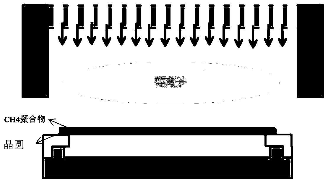
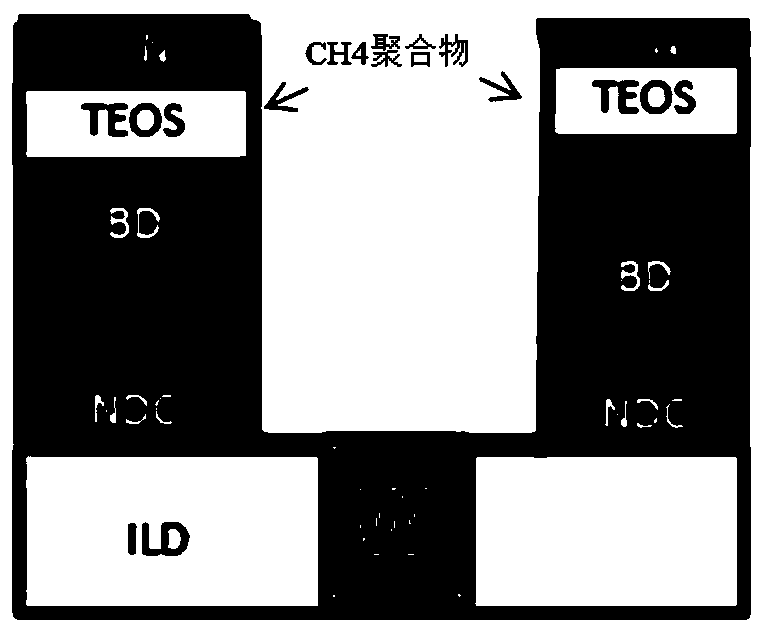
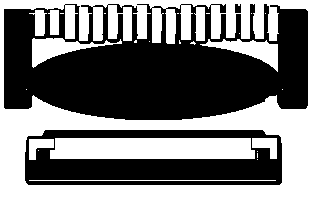
[0045] refer to figure 2 , figure 2 It is a schematic structural diagram showing a polymer protective layer formed on the surface of the semiconductor structure in the present invention. Step 2 of the present invention forms a polymer protective layer on the surface of the semiconductor structure while forming the polymer protective layer on the surface of the wafer.

[0046] The present invention provides a method for improving the residual microparticles on the wafer surface, referring to Figure 7 , Figure 7 It is shown as a flow chart of the method for improving the microparticle residue on the wafer surface of the present invention. The method described in this embodiment to improve the residual microparticles on the surface of the wafer comprises the following steps:

[0047] Step 1: Provide a plasma reactive etching chamber and a wafer located in the plasma reactive etching chamber, the wafer is provided with a semiconductor structure, and the semiconductor struc...

Embodiment 3

[0057] refer to figure 2 , figure 2 It is a schematic structural diagram showing a polymer protective layer formed on the surface of the semiconductor structure in the present invention. Step 2 of the present invention forms a polymer protective layer on the surface of the semiconductor structure while forming the polymer protective layer on the surface of the wafer.

[0058] The present invention provides a method for improving the residual microparticles on the wafer surface, referring to Figure 7 , Figure 7 It is shown as a flow chart of the method for improving the microparticle residue on the wafer surface of the present invention. The method described in this embodiment to improve the residual microparticles on the surface of the wafer comprises the following steps:

[0059] Step 1: Provide a plasma reactive etching chamber and a wafer located in the plasma reactive etching chamber, the wafer is provided with a semiconductor structure, and the semiconductor struc...


PUM


Abstract

The invention provides a method for improving residual microparticles on the surface of a wafer. The method comprises the following steps of firstly, providing a plasma reaction etching cavity and a wafer positioned in the plasma reaction etching cavity, arranging a semiconductor structure on the wafer, and ensuring that the semiconductor structure is in a process state that etching of a first layer of metal groove is finished; secondly, forming a polymer protective layer on the surface of the wafer; thirdly, introducing a plasma source into the plasma reaction etching cavity to remove chargeson the surface of the wafer; and finally, stopping introducing the plasma source, and standing the wafer. According to the invention, after the completion of the groove etching process on the first layer of metal groove, a protective layer is formed on the surface of the wafer by using a gas source for depositing a polymer in the subsequent process. After that, microparticles in the cavity are adsorbed and brought out of the etching cavity by using a macromolecular gas source assisted destaticizing process in the subsequent destaticizing process, so that particle attachments caused in the wafer decharging process are solved.

Description

technical field [0001] The invention relates to the field of semiconductor manufacturing, in particular to a method for improving microparticle residues on the wafer surface. Background technique [0002] The first metal connection layer is the first metal layer connected to the metal tungsten contact hole plug, which is a single damascene structure, and its main function is to locally connect and lead out the front-end devices. With the gradual development of integrated circuit technology nodes beyond 90nm, the etching technology of the first metal connection layer has also developed from the traditional two-pass etching technology of photoresist as a barrier layer, and adopts a "sandwich" structure multi-layer mask one-stop Etching technology, and then to the one-stop discrete immediate etching technology using metal TiN as a barrier layer. [0003] When the etching process is performed using metal TiN etc. as the hard mask technology of the first layer of metal trenches,...

Claims


Application Information

Patent Timeline
IPC IPC(8): H01L21/3105
CPCH01L21/31058H01J37/32715H01J37/32082H01L21/6831H01J2237/022H01J2237/2007H01J2237/3341H01L21/67069
Inventor 聂钰节聂珊珊钱洋洋
Owner SHANGHAI HUALI MICROELECTRONICS CORP
Why Eureka
Try Eureka