
Self-designed low-noise amplifying circuit experimental device

A technology of low noise amplification and experimental device, applied in the field of electronics, to achieve the effects of easy processing, high safety and low cost

Inactive Publication Date: 2019-11-19
DALIAN MARITIME UNIVERSITY
View PDF8 Cites 0 Cited by
  • Summary
  • Abstract
  • Description
  • Claims
  • Application Information

AI Technical Summary

Problems solved by technology

Most of the current RF experiment boards in the laboratory are for passive devices, and there are almost no experiment boards for RF active devices.

Method used


Image

  • Self-designed low-noise amplifying circuit experimental device
  • Self-designed low-noise amplifying circuit experimental device
  • Self-designed low-noise amplifying circuit experimental device

Examples


Embodiment

[0024] The following takes the ATF54143 low-noise amplifier chip as an example, and uses a 1.5mm FR4 dielectric board for design and implementation under the condition of a frequency of 900MHz. The technical solutions in the embodiments of the present invention are described clearly and completely with reference to the drawings in the embodiments of the present invention. :

[0025] Step 1: First measure the static operating point of the low-noise amplifier chip 21, and determine the resistance of the DC bias resistor through the static operating point: the resistance of the first DC bias resistor 2411 is 82 ohms, the second DC bias The resistance value of the resistor 2412 is 620 ohms, and the resistance value of the third DC bias resistor 2413 is 33 ohms; the second step: add a radio frequency choke circuit between the AC and DC paths, and introduce a DC blocking capacitor, a choke inductance and a bypass. Their parameters are: the capacitance value of the DC blocking capaci...


PUM


Abstract

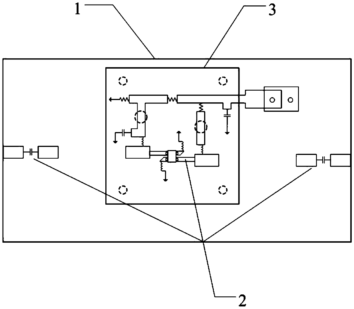
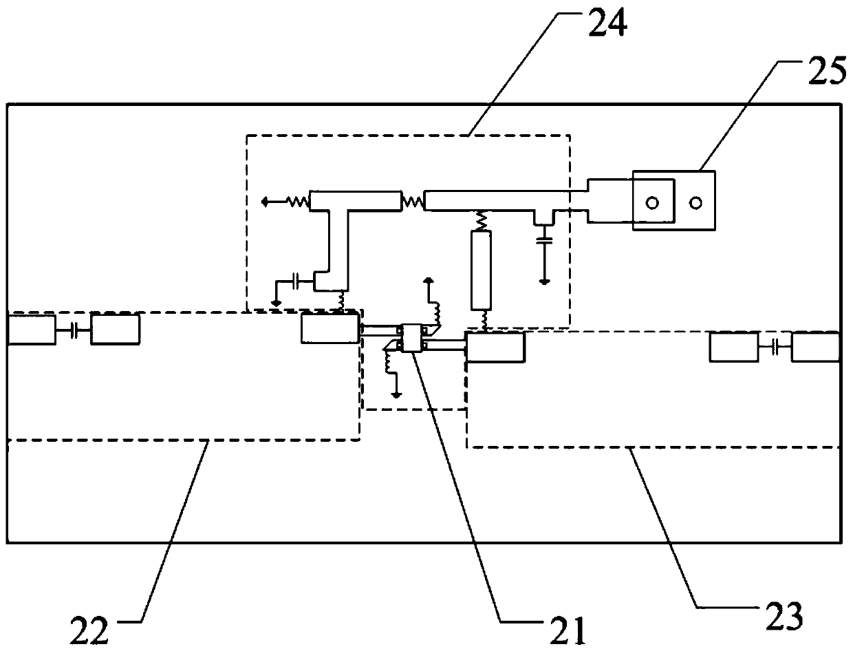
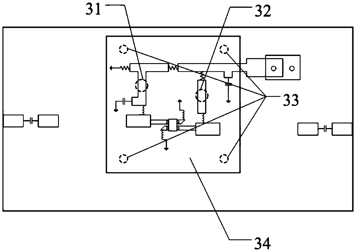
The present invention discloses a self-designed low-noise amplifying circuit experimental device. The self-designed low-noise amplifying circuit experimental device comprises a dielectric plate, a low-noise amplifying circuit and a DC bias circuit protective cover; the low-noise amplifying circuit comprises low-noise amplifying chips, an input matching circuit, an output matching circuit, a DC bias circuit and a 5V plug-in power supply module; and the DC bias circuit protective cover comprises a chip gate source voltage measuring point and a chip drain source voltage measuring point. Accordingto the self-designed low-noise amplifying circuit experimental device provided by the present invention, a plurality of low-noise amplifying chips are available for selection; and after the input-output matching circuits are determined through software simulation, the matching circuits can be pasted by using double-lead copper foil in the input matching design area and the output matching designarea, and lengths of the series and parallel matching microstrip lines are adjusted through actual measurement to achieve input and output matching, so that reducing noise in the signal and amplifyingthe signal can be realized.

Description

technical field [0001] The invention belongs to the technical field of electronics, and in particular relates to a self-designed low-noise amplifying circuit experimental device. Background technique [0002] With the rapid development of wireless communication technology, radio frequency technology has gradually become the focus of attention. The radio frequency circuit is mainly divided into active circuit and passive circuit. The low noise amplifier circuit is an important radio frequency active circuit. Its function is to amplify the weak signal received by the antenna from the air and reduce noise interference for system demodulation. out information data. It is generally used as a high-frequency or intermediate-frequency preamplifier for various radio receivers, and an amplifier circuit for high-sensitivity electronic detection equipment. [0003] In recent years, various colleges and universities have offered RF experimental courses, but they are limited to measurin...

Claims


Application Information

Patent Timeline
Patent Type & Authority Applications(China)
IPC IPC(8): G09B23/18
CPCG09B23/183
Inventor 刘宏梅张妍郭晓建房少军王钟葆傅世强
Owner DALIAN MARITIME UNIVERSITY
Learn More