Method for silk-screening solder resist ink on PCB with small-spacing bonding pads

A technology of solder mask ink and screen printing ink, which is applied in the secondary treatment of printed circuits, sustainable manufacturing/processing, climate sustainability, etc. short circuit effect

Active Publication Date: 2019-11-19
惠州美锐电子科技有限公司
View PDF4 Cites 8 Cited by
  • Summary
  • Abstract
  • Description
  • Claims
  • Application Information

AI Technical Summary

Problems solved by technology

Solder resist ink (that is, oil bridge) needs to be made between adjacent pads on the PCB to avoid short circuit between adjacent pads during patching. For some PCBs with too small pad spacing, the general screen printing process is used to make resist When soldering the ink layer, the oil bridge is easy to be side-eroded, which will cause the oil bridge to fall off, affect the quality of the PCB, and even directly cause the entire board to be scrapped after placement

Method used


Image

  • Method for silk-screening solder resist ink on PCB with small-spacing bonding pads
  • Method for silk-screening solder resist ink on PCB with small-spacing bonding pads
  • Method for silk-screening solder resist ink on PCB with small-spacing bonding pads

Examples


Embodiment 1

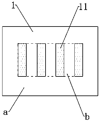
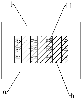
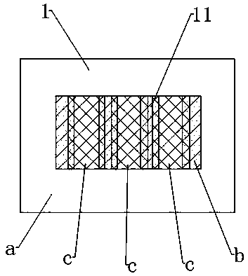
[0030] refer to Figure 1~7 A method for screen printing solder resist ink on PCB with small pitch pads, used for silk screen printing of solder resist ink on the surface of PCB when the pitch of pads is small. The solder resist ink is screen-printed on the surface of the PCB 1 twice, and the solder resist ink is screen-printed on the pad area b for the first time (the pad area b includes the surfaces of multiple adjacent pads 11 and the PCB between adjacent pads. Surface area), mainly to complete the silk screen printing of solder resist ink (ie, oil bridge) between 11 adjacent pads; secondly, silk screen solder resist ink on the area a outside the pad area on the PCB, and complete the entire surface of the PCB requires silk screen solder resist Silkscreen for ink placement.

[0031] The schematic diagram of the PCB surface structure before the first silk screen printing solder resist ink is as follows figure 1 As shown, the first screen printing solder resist ink includes ...


PUM


Abstract

The invention discloses a method for silk-screening solder resist ink on a PCB with small-spacing bonding pads. The method comprises the steps of: performing silk-screening the solder resist ink on the surface of a PCB twice, performing silk-screening the solder resist ink in a bonding pad area for the first time, and performing silk-screening the solder resist ink in a position outside the bonding pad area on the PCB for the second time, wherein the first silk-screen printing of the solder resist ink comprises the following steps of: S1, silk-screen printing of ink: silk-screen printing of ink is performed on a position between the adjacent bonding pads in the bonding pad area, and the silk-screen printing ink area is expanded to the bonding pads; S2, pre-drying treatment: the silk-screenprinting ink is dried to be a non-sticky object; S3, exposure processing: ink silk-screened in the area between the bonding pads is exposed, and the exposure area is expanded to the bonding pads; S4,developing treatment: the oil ink on the bonding pads and on the outer side of the bonding pads is removed through a developing solution; S5, curing treatment: curing treatment is performed on the ink left by development between the bonding pads and on the bonding pads; and S6, polishing treatment: polishing and removing the ink cured on the bonding pads are performed. The method for silk-screening solder resist ink on the PCB with small-spacing bonding pads is used for PCB silk-screen solder resist ink of small-spacing bonding pads.

Description

technical field [0001] The invention relates to the technical field of PCB production and processing, in particular to a method for PCB silk screen printing solder resist ink for small-pitch pads. Background technique [0002] PCB (Printed Circuit Board, printed circuit board) is a commonly used component in electrical equipment. Usually, various components need to be mounted or inserted on the PCB to form electrical functional modules to realize various functions of electrical equipment. After the circuit on the PCB is completed, it is necessary to screen-print solder resist ink on the surface to protect the circuit on the PCB and avoid short circuits between pads when components are mounted. With the ever-changing changes, the SMT components are getting smaller and smaller, and the PIN pins of the components are getting denser. These directly affect the structure of the PCB board, resulting in smaller and smaller spacing between the pads on the PCB. Solder resist ink (tha...

Claims


Application Information

Patent Timeline
Patent Type & Authority Applications(China)
IPC IPC(8): H05K3/28
CPCH05K3/28Y02P70/50
Inventor 陈超兵
Owner 惠州美锐电子科技有限公司
Why Eureka
Try Eureka