
Eureka
For R&D, Eureka makes reading and utilizing patents & technical documents easy.
Eureka AIR
Designed for self-driven R&D workflows. Generate viable solutions, solve complex R&D challenges, empower your innovation with AI.

Eureka Materials
Designed for material experts only. Revolutionize your material R&D, from search, analyze, to developing new materials.

TechResearch
Generate reliable direction feasibility study reports for your R&D in just a few steps.

TechSeek
Discover and master advanced knowledge NOW. Basics, ideas, possibilities, all at once.

TechMind
As an expert in R&D Theories, TechMind can generates customized viable solutions instantly.

TechRisk
Analyze your overall solution with one click, know your potential R&D risks in advance.

TechMonitor
Get weekly tech updates, stay abreast of the latest tech innovations and key insights.
1.5T SONOS flash memory device and process method thereof
A 1.5TSONOS and flash memory device technology, which is applied in the manufacture of electrical solid state devices, semiconductor devices, semiconductor/solid state devices, etc., can solve the problems of thickness limitation, occupation, loss of large chip area, etc., and achieve the effect of facilitating process integration
- Summary
- Abstract
- Description
- Claims
- Application Information
AI Technical Summary
Problems solved by technology
Method used
Image


Examples
Embodiment Construction
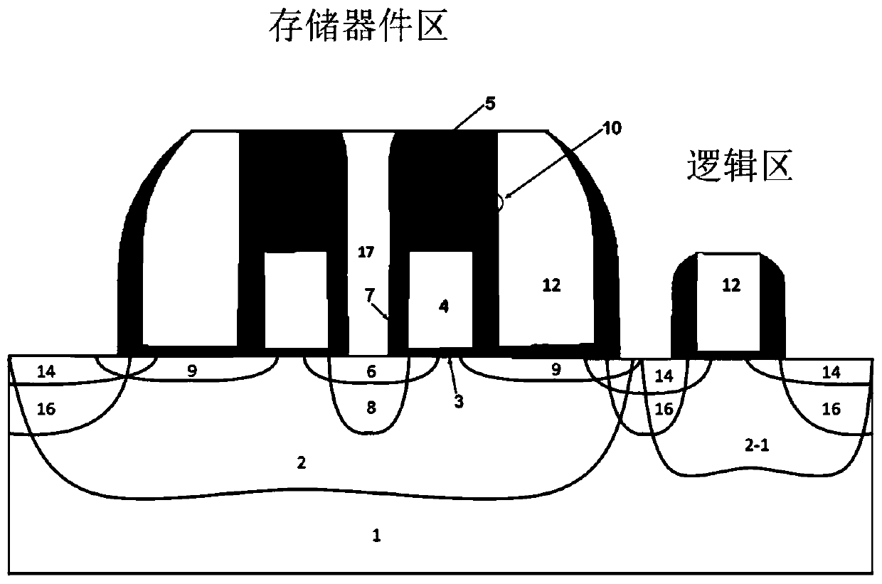
[0073] The 1.5T SONOS flash memory device described in the present invention is as Figure 24 shown, including:
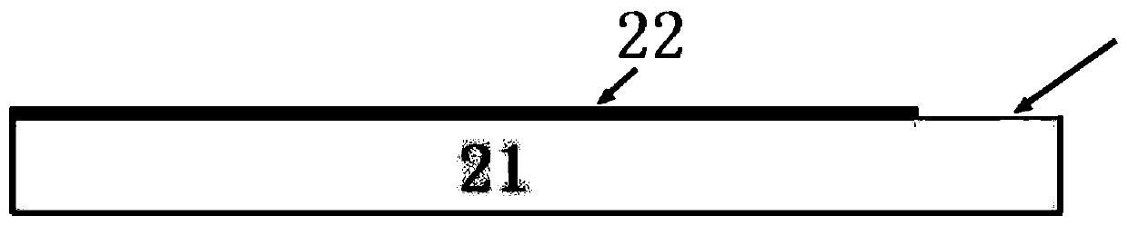
[0074] A semiconductor substrate, such as a silicon substrate, is generally P-type silicon, and is divided into a memory cell area and a logic area on the semiconductor substrate 21; the memory cell area is located in a P well in the semiconductor substrate, so The logic region is located in the CMOS tube well region in the semiconductor substrate (the illustration of each implantation region in the substrate is omitted in this figure, refer to figure 1 The arrangement of the injection regions in the figure 1 The structure and arrangement of each implanted region in the substrate are the same; and the process steps also omit the labeling of each implanted region in the substrate); figure 2 The P well on the left is used to form the memory cell area, and the CMOS well on the right is used to form the logic area and make the logic body. The P well is not in conta...
PUM
 Abstract
Description
Claims
Application Information
 - R&D Engineer
- R&D Manager
- IP Professional
- Industry Leading Data Capabilities
- Powerful AI technology
- Patent DNA Extraction
Browse by: Latest US Patents, China's latest patents, Technical Efficacy Thesaurus, Application Domain, Technology Topic, Popular Technical Reports.
© 2024 PatSnap. All rights reserved.Legal|Privacy policy|Modern Slavery Act Transparency Statement|Sitemap|About US| Contact US: help@patsnap.com